
Part Datasheet Search > Logic Gates > CD4081 Pinout Diagram
Images are for reference
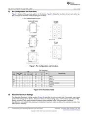
CD4081 Pinout Diagram
| Part Series: | CD4081 Series |
| Category: | Logic Gates |
| Description: | AND Gate 4Element 2IN CMOS 14Pin PDIP Tube |
| Document: | CD4081BNSR Application Note (60 Pages) |
CD4081 Logic Gates Pinout Diagram
Part Datasheet PDF Search
72,405,303 Parts Datasheet PDF, Update more than 5,000 PDF files ervery day.