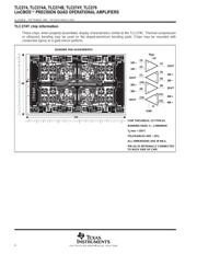
Part Datasheet Search > Operational Amplifiers(General Purpose) > TLC274 Pinout Diagram
Images are for reference

TLC274 Pinout Diagram

Part Series:TLC274 Series
Category:Operational Amplifiers(General Purpose)
Description:Operational Amplifier, Quad, 4 Amplifier, 1.7MHz, 3.6V/µs, 3V to 16V, SOIC, 14Pins
Document:TLC274CDR Datasheet PDF (53 Pages)

TLC274 Operational Amplifiers(General Purpose) Pinout Diagram

TLC274CDR Specifications

TYPE
DESCRIPTION
Mounting Style
Surface Mount
Number of Pins
14 Pin
Operating Voltage
3V ~ 16V
Case/Package
SOIC-14
Output Current
≤30 mA
show more

TLC274CDR Function Overview

description
The TLC274 and TLC279 quad operational amplifiers combine a wide range of input offset voltage grades with low offset voltage drift, high input impedance, low noise, and speeds approaching that of general-purpose BiFET devices.
Trimmed Offset Voltage:
   TLC279. . . 900 µV Max at 25°C, VDD= 5 V
Input Offset Voltage Drift...Typicall 0.1 µV/Month, Including the First 30 Days
Wide Range of Supply Voltages Over Specified Temperature Range:
    0°C to 70°C...3 V to 16 V
    −40°C to 85°C...4 V to 16 V
   −55°C to 125°C...4 V to 16 V
Single-Supply Operation
Common-Mode Input Voltage Range Extends Below the Negative Rail (C-Suffix and I-Suffix Versions)
Low Noise...Typically 25 nV/√Hz at f = 1 kHz
Output Voltage Range Includes Negative Rail
High Input Impedance...1012ΩTyp
ESD-Protection Circuitry
Small-Outline Package Option Also Available in Tape and Reel
Designed-In Latch-Up Immunity
show more
Part Datasheet PDF Search
72,405,303 Parts Datasheet PDF, Update more than 5,000 PDF files ervery day.