
Part Datasheet Search > Voltage Regulators > Linear Technology > LT1074HVIT7#06PBF Datasheet PDF > LT1074HVIT7#06PBF Application Note Pages 1/32
LT1074HVIT7#06PBFDatasheet PDF
Page:
of 32 Go
If the format of the manual is confusing, please download and read the original PDF file.
Application Note 35
AN35-1
an35f
August 1989
Step-Down Switching Regulators
Jim Williams
A substantial percentage of regulator requirements
involve stepping down the primary voltage. Although
linear regulators can do this, they cannot achieve the
effi ciency of switching based approaches
1
. The theory
supporting step-down (“buck”) switching regulation is
well established, and has been exploited for some time.
Convenient, easily applied ICs allowing implementation
of practical circuits are, however, relatively new. These
devices permit broad application of step-down regulation
with minimal complexity and low cost. Additionally, more
complex functions incorporating step-down regulation
become realizable.
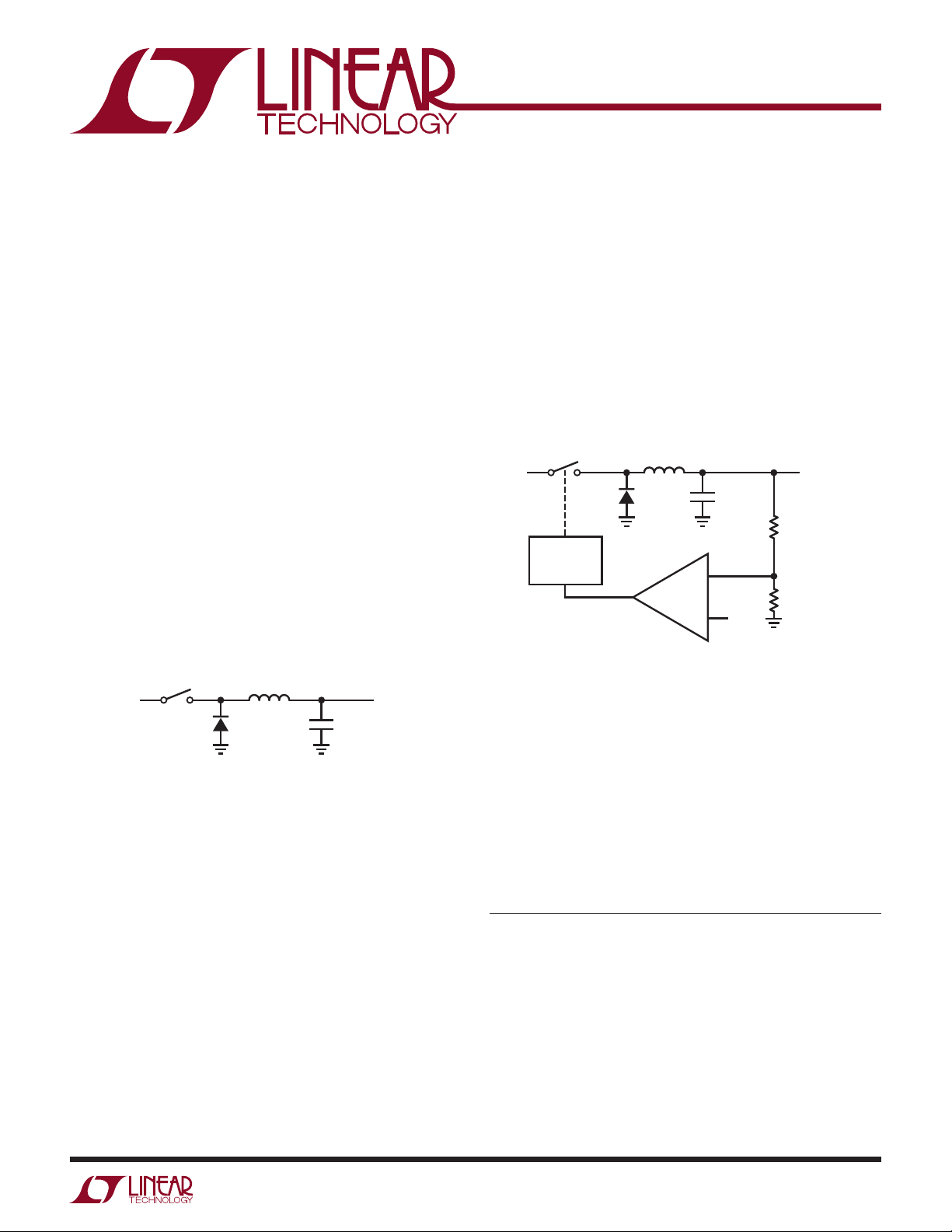
Basic Step Down Circuit
Figure 1 is a conceptual voltage step-down or “buck”
circuit. When the switch closes the input voltage appears
at the inductor. Current fl owing through the inductor-ca-
pacitor combination builds over time. When the switch
IN OUT
AN35 F01
Figure 1. Conceptual Voltage Step-Down (“Buck”) Circuit
opens current fl ow ceases and the magnetic fi eld around
the inductor collapses. Faraday teaches that the voltage
induced by the collapsing magnetic fi eld is opposite to the
originally applied voltage. As such, the inductor’s left side
heads negative and is clamped by the diode. The capaci-
tors accumulated charge has no discharge path, and a DC
potential appears at the output. This DC potential is lower
than the input because the inductor limits current during
the switch’s on-time. Ideally, there are no dissipative ele-
ments in this voltage step-down conversion. Although the
output voltage is lower than the input, there is no energy
lost in this voltage-to-current-to-magnetic fi eld-to-cur-
rent-to-charge-to-voltage conversion. In practice, the
circuit elements have losses, but step-down effi ciency is
still higher than with inherently dissipative (e.g., voltage
divider) approaches. Figure 2 feedback controls the basic
circuit to regulate output voltage. In this case switch on-
time (e.g., inductor charge time) is varied to maintain the
output against changes in input or loading.
IN
REGULATED
OUTPUT
V
REF
AN35 F02
–
+
PULSE
WIDTH
MODULATOR
Figure 2. Conceptual Feedback Controlled Step-Down Regulator
Practical Step-Down Switching Regulator
Figure 3, a practical circuit using the LT
®
1074
2
IC regulator,
shows similarities to the conceptual regulator. Some new
elements have also appeared. Components at the LT1074’s
“V
COMP
” pin control the IC’s frequency compensation,
stabilizing the feedback loop. The feedback resistors are
selected to force the “feedback” pin to the device’s internal
2.5V reference value. Figure 4 shows operating waveforms
for the regulator at V
IN
= 28V with a 5V, 1A load.
L, LT, LTC, LTM, Linear Technology and the Linear logo are registered
trademarks of Linear Technology Corporation. All other trademarks are the
property of their respective owners.
Note 1: While linear regulators cannot compete with switchers, they can
achieve signifi cantly better effi ciencies than generally supposed. See LTC
Application Note 32, “High Effi ciency Linear Regulators,” for details.
Note 2: See Appendix A for details on this device.
Part Datasheet PDF Search
72,405,303 Parts Datasheet PDF, Update more than 5,000 PDF files ervery day.