Product Details
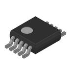
●The AD5310R/AD5311R, members of the _nano_DAC™ family, are low power, single-channel, 10-bit buffered voltage-out DACs. The devices include a 2.5 V, 2 ppm/°C internal reference. The output span can be programmed to be 0 V to VREF or 0 V to 2 ×VREF. All devices operate from a single 2.7 V to 5.5 V supply and are guaranteed monotonic by design. The devices are available in 10-lead MSOP packages.
●The AD5310R/AD5311R also incorporate a power-on reset circuit that ensures that the DAC output powers up to zeroscale and remains there until a valid write takes place. The device contains a power-down feature that reduces the current consumption of the device to 2 μA at 5 V while in power-down mode.
●The AD5310R/AD5311R use a versatile SPI or I2C interface, including an asynchronous RESET pin and a VLOGIC pin, allowing 1.8 V compatibility.
●PRODUCT HIGHLIGHTS
● 1. High Relative Accuracy (INL).
●±0.5 LSB maximum.
● 2. Low Drift 2.5 V On-Chip Reference.
●5 ppm/°C maximum temperature coefficient.
●APPLICATIONS
● Process controls
● Data acquisition systems
● Digital gain and offset adjustment
● Programmable voltage sources
● Optical modules
●### Features and Benefits
● High relative accuracy (INL):
●±0.5 LSB maximum
● Low drift 2.5 V reference:
●2 ppm/°C typical
● Selectable span output:
●2.5 V or 5 V
● Total unadjusted error (TUE):
●0.06% of FSR maximum
●Offset error: ±1.5 mV maximum
●Gain error: ±0.05 % of FSR maximum
● Low glitch: 0.1 nV-sec
● High drive capability: 20 mA
● Low power: 1.2 mW at 3.3 V
● Independent logic supply:
●1.8 V to 5.5 V
● Wide operating temperature range:
●−40°C to +105°C
● Robust 4 kV ESD protection


