Product Details
●The AD5686R _nano_DAC+™ is a quad, 16-bit, rail-to-rail, voltage output DAC. The device includes a 2.5V, 2ppm/˚C internal reference (enabled by default) and a gain select pin giving a full-scale output of 2.5V (gain=1) or 5V (gain=2).
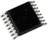
●The device operates from a single 2.7 V to 5.5 V supply, is guaranteed monotonic by design and exhibits less than 0.1% FSR gain error and 1.5mV offset error performance. The device is available in a 3mm X 3mm LFCSP and a TSSOP package.
●The AD5686R also incorporates a power-on-reset circuit and a RSTSEL pin that ensures the DAC outputs power up to zero-scale or midscale, and remain there until a valid write takes place. Each device contains a per-channel power-down feature that reduces the current consumption of the device to 4 uA at 3 V while in power-down mode.
●The AD5686R employs a versatile SPI interface that operates at clock rates up to 50 MHz and includes a VLOGIC pin intended for 1.8V/3V/5V logic.
●Product Highlights
● 1. High Relative Accuracy: AD5686R (16-bit): ±2LSB INL max
● 2. Low drift on-chip reference: 2.5 V, 2 ppm/°C temperature drift.
● 3. Two package options: 3mm × 3mm 16 lead LFCSP or 16 lead TSSOP
●Applications
● Optical transceivers
● Base-station power amplifiers
● Process control (PLC I/O cards)
● Industrial automation
● Data acquisition systems
●### Features and Benefits
● High relative accuracy (INL): ±2 LSB maximum at 16-bits
● Low drift 2.5 V reference:: 2 ppm/°C typical
● Tiny package: 3 mm × 3 mm, 16-lead LFCSP or TSSOP
● Total unadjusted error (TUE): 0.1% of FSR maximum
● Offset error: 1.5 mV maximum
● Gain error: 0.1 % of FSR maximum
● See data sheet for additional features
●AD5686R-EP supports defense and aerospace applications (AQEC standard)
● Download AD5686R-EP Data Sheet (pdf)
● Temperature range: −55°C to +125°C
● Controlled manufacturing baseline
● 1 assembly/test site
● 1 fabrication site
● Enhanced product change notification
● Qualification data available on request
● V62/14335 DSCC Drawing Number


