Part Datasheet Search > Digital to Analog > ADI > AD660SQ Datasheet PDF
AD660SQ Datasheet PDF - ADI
| Manufacturer: | ADI |
| Category: | Digital to Analog |
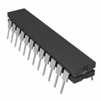
| Case Package: | CDIP-24 |
| Description: | DAC 1CH R-2R/Current Steering 16Bit 24Pin CDIP Tube |
| Documentation: | AD660SQ Datasheet (20 Pages)Pinout Diagram on8 PageHot Package Outline Dimension on18 Page Part Numbering System on19 Page |
| Pictures: |
AD660SQ Datasheet PDF
ADatasheet has not yet included the datasheet for AD660SQ
If necessary, please send a supplementary document request to the administrator

AD660SQ Datasheet PDF (20 Pages)
AD660SQ Specifications
| TYPE | DESCRIPTION |
|---|---|
| Mounting Style | Through Hole |
| Number of Pins | 24 Pin |
| Case/Package | CDIP-24 |
| Number of Outputs | 1 Output |
| Number of Channels | 1 Channel |
| Number of Bits | 16 Bit |
| Power Dissipation | 0.625 W |
| Sample Rate | 167 ksps |
| Resolution (Bits) | 16.0 Bit |
| Operating Temperature (Max) | 125 ℃ |
| Operating Temperature (Min) | -55 ℃ |
| Power Dissipation (Max) | 625 mW |
| Supply Voltage (Max) | 16.5 V |
| Supply Voltage (Min) | 13.5 V |
AD660SQ Size & Package
| TYPE | DESCRIPTION |
|---|---|
| Product Lifecycle Status | Active |
| Packaging | Tube |
| Size-Height | 3.56 mm |
AD660SQ Environmental
AD660SQ Export Classifications
AD660SQ Function Overview
Product Details
●The AD660 DACPORT® is a complete 16-bit monolithic digital-to-analog converter with an on-board voltage reference, double-buffered latches, and an output amplifier. It is manufactured on the Analog Devices, Inc., BiMOS II process. This process allows the fabrication of low power CMOS logic functions on the same chip as high precision bipolar linear circuitry.
●The AD660 architecture ensures 15-bit monotonicity over time and temperature. Integral and differential nonlinearity is main-tained at ±0.003% maximum. The on-chip output amplifier provides a voltage output settling time of 10 μs to within ½ LSB for a full-scale step.
●The AD660 has an extremely flexible digital interface. Data can be loaded into the AD660 in serial mode or as two 8-bit bytes. This is made possible by two digital input pins that have dual functions. The serial mode input format is pin selectable to be MSB or LSB first. The serial output pin allows the user to daisy-chain several AD660 devices by shifting the data through the input latch into the next DAC, thus minimizing the number of control lines required to SIN, CS and LDAC. The byte mode input format is also flexible in that the high byte or low byte data can be loaded first. The double buffered latch structure eliminates data skew errors and provides for simultaneous updating of DACs in a multiDAC system.
●The AD660 is available in five grades. AN and BN versions are specified from −40°C to +85°C and are packaged in a 24-lead300 mil plastic DIP. AR and BR versions are also specified from −40°C to +85°C and are packaged in a 24-lead SOIC. The SQ version is packaged in a 24-lead 300 mil CERDIP package and is also available compliant to MIL-STD-883. Refer to theAD660SQ/883B military data sheet for specifications and test conditions.
●Product Highlights
● 1. The AD660 is a complete 16-bit DAC, with a voltage reference, double-buffered latches, and an output amplifier on a single chip.
● 2. The internal buried Zener reference is laser trimmed to 10.000 V with a ±0.1% maximum error and a temperature drift performance of ±15 ppm/°C. The reference is available for external applications.
● 3. The output range of the AD660 is pin programmable and can be set to provide a unipolar output range of 0 V to 10 Vor a bipolar output range of −10 V to +10 V. No external components are required.
● 4. The AD660 is both dc and ac specified. DC specifications include ±1 LSB INL and ±1 LSB DNL errors. AC specifications include 0.009% THD + N and 83 dB SNR.
● 5. The double-buffered latches on the AD660 eliminate data skew errors and allow simultaneous updating of DACs inmultiDAC applications.
● 6. The clear function can asynchronously set the output to 0 V regardless of whether the DAC is in unipolar or bipolar mode.
● 7. The output amplifier settles within 10 μs to ±½ LSB for a full-scale step and within 2.5 μs for a 1 LSB step over temperature. The output glitch is typically 15 nV-s when a full-scale step is loaded.
●Data Sheet, Rev. B, 6/08
●### Features and Benefits
● Complete 16-Bit D/A Function
●On-Chip Output Amplifier
●On-Chip Buried Zener Voltage Reference
● ±1LSB Integral Linearity
● 15-Bit Monotonic over Temperature
● Microprocessor Compatible
●Serial or Byte Input
●Double Buffered Latches
●Fast (40 ns) Write Pulse
● Asynchronous Clear (to 0 V) Function
● Serial Output Pin Facilitates Daisy Chaining
● Unipolar or Bipolar Output
● Low Glitch: 15 nV-s
● Low THD+N: 0.009%
show more
AD660SQ Documents
AD660 Documents
ADI
Digital to Analog Converter, 16Bit, 167KSPS, Serial, ± 13.5V to ± 16.5V, WSOIC, 24Pins
ADI
ANALOG DEVICES AD660ANZ Digital to Analog Converter, 16Bit, 167KSPS, Serial, ± 13.5V to ± 16.5V, DIP, 24Pins
ADI
ANALOG DEVICES AD6600ASTZ Analog to Digital Converter, 11Bit, 20MSPS, Single, 4.75V, 5.25V, LQFP
ADI
ANALOG DEVICES AD660BRZ Digital to Analog Converter, 16Bit, 167KSPS, Serial, ± 13.5V to ± 16.5V, WSOIC, 24Pins
Part Datasheet PDF Search
Example: STM32F103
72,405,303 Parts Datasheet PDF, Update more than 5,000 PDF files ervery day.

