Product Details
●The AD7927 is a 12-bit, high speed, low power, 8-channel, successive approximation ADC. The part operates from a single 2.7 V to 5.25 V power supply and features throughput rates up to 200 kSPS. The part contains a low noise, wide bandwidth track-and-hold amplifier that can handle input frequencies in excess of 8 MHz.
●The conversion process and data acquisition are controlled using CS and the serial clock signal, allowing the device to easily interface with microprocessors or DSPs. The input signal is sampled on the falling edge of CS and the conversion is also initiated at this point. There are no pipeline delays associated with the part.
●The AD7927 uses advanced design techniques to achieve very low power dissipation at maximum throughput rates. At maximum throughput rates, the AD7927 consumes 1.2 mA maximum with 3 V supplies; with 5 V supplies, the current consumption is 1.5 mA maximum.
●Through the configuration of the control register, the analog input range for the part can be selected as 0 V to REFIN or 0 V to 2 × REFIN, with either straight binary or twos complement output coding. The AD7927 features eight single-ended analog inputs with a channel sequencer to allow a preprogrammed selection of channels to be converted sequentially.
●The conversion time for the AD7927 is determined by the SCLK frequency, as this is also used as the master clock to control the conversion. The conversion time may be as short as 800 ns with a 20 MHz SCLK.
●Product Highlights
● High Throughput with Low Power Consumption. The AD7927 offers up to 200 kSPS throughput rates. At the maximum throughput rate with 3 V supplies, the AD7927 dissipates 3.6 mW of power maximum.
● Eight Single-Ended Inputs with a Channel Sequencer. A consecutive sequence of channels can be selected on which the ADC cycles and converts.
● Single-Supply Operation with VDRIVE Function. The AD7927 operates from a single 2.7 V to 5.25 V supply. The VDRIVE function allows the serial interface to connect directly to either 3 V or 5 V processor systems independent of AVDD.
● Flexible Power/Serial Clock Speed Management. The conversion rate is determined by the serial clock, allowing the conversion time to be reduced through the serial clock speed increase. The part also features various shutdown modes to maximize power efficiency at lower throughput rates. Current consumption is 0.5 μA maxi-mum when in full shutdown.
● No Pipeline Delay. The part features a standard successive approximation ADC with a CS input pin, which allows for accurate control of each sampling instant.
●### Features and Benefits
● Fast throughput rate: 200 kSPS
● Specified for AVDD of 2.7V to 5.25V
● Low power
●3.6 mW maximum at 200 kSPS with 3 V supply
●7.5 mW maximum at 200 kSPS with 5 V supply
● 8 (single-ended) inputs with sequencer
● Flexible power/serial clock speed management
● Wide input bandwidth
●70 dB minimum SINAD at 50 kHz input frequency
● No pipeline delays
● High speed serial interface SPI™-, QSPI™-, MICROWIRE™-, DSP-compatible
● Shutdown mode: 0.5 μA maximum
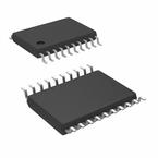
● 20-lead TSSOP
● Qualified for Automotive


