Product Details
●The AD9262 is a dual, 16-bit analog-to-digital converter (ADC) based on a continuous time sigma-delta (Σ-Δ) architecture that achieves -87 dB of dynamic range over a 10 MHz input bandwidth. The integrated features and characteristics unique to the continuous time Σ-Δ architecture significantly simplify its use and minimize the need for external components.
●The AD9262 has a resistive input impedance that significantly relaxes the requirements of the driver amplifier. In addition, a 32× oversampled 5th-order continuous time loop filter significantly attenuates out of band signals and aliases, reducing the need for external filters at the input.
●An external clock input or the integrated integer-N PLL provides the 640 MHz internal clock needed for the oversampled continuous time Σ-Δ modulator. On-chip decimation filters and sample rate converters reduce the modulator data rate from 640 MSPS to a user-defined output data rate between 30 MSPS to 160 MSPS, enabling a more efficient and direct interface.
●The AD9262 incorporates an integrated dc correction and quadrature estimation block that corrects for gain and phase mismatch between the two channels. This functional block proves invaluable in complex signal processing applications such as direct conversion receivers.
●The digital output data is presented in offset binary, Gray code, or twos complement format. A data clock output (DCO) is provided to ensure proper timing with the receiving logic. The AD9262 has the added feature of interleaving Channel A and Channel B data onto one 16-bit bus, simplifying on-board routing.
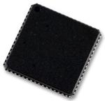
●The ADC is available in three different bandwidth options of 2.5 MHz, 5 MHz, and 10 MHz, and operates on a 1.8 V analog supply and a 1.8 V to 3.3 V digital supply, consuming 600 mW. The AD9262 is available in a 64-lead LFCSP and is specified over the industrial temperature range (−40°C to +85°C).
●Product Highlights
● 1. Continuous time Σ-Δ architecture efficiently achieves high dynamic range and wide bandwidth.
● 2. Passive input structure reduces or eliminates the requirements for a driver amplifier.
● 3. An oversampling ratio of 32× and high order loop filter provide excellent alias rejection reducing or eliminating the need for antialiasing filters.
● 4. An integrated decimation filter, sample rate converter, PLL clock multiplier, and voltage reference provide ease of use.
● 5. Operates from a single 1.8 V analog power supply and 1.8 V to 3.3 V output supply.
● 6. A standard serial port interface (SPI) supports various product features and functions.
●Applications
● Baseband quadrature receivers: CDMA2000, WCDMA, multicarrier GSM/EDGE, 802.16x, and LTE
● Quadrature sampling instrumentation
● Medical equipment
● Radio detection and ranging (RADAR)
●### Features and Benefits
● SNR: 83 dB (85 dBFS) to 10 MHz input
● SFDR: 87 dBc to 10 MHz input
● Noise figure: 15 dB
● Input impedance: 1 kΩ
● Power: 600 mW
● 1.8 V analog supply operation
● 1.8 V to 3.3 V output supply
● Selectable bandwidth
●2.5 MHz/5 MHz/10 MHz real
●5 MHz/10 MHz/20 MHz complex
● Dual channel modulator only version available (AD9267)
● Output data rate: 30 MSPS to
●160 MSPS
● See data sheet for additional features


