●NOTE: Some device/package combinations are obsolete and are described and shown here for reference only. See our web site for product availability.
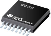
●The ADC12130, ADC12132 and ADC12138 are 12-bit plus sign successive approximation Analog-to-Digital converters with serial I/O and configurable input multiplexer. The ADC12132 and ADC12138 have a 2 and an 8 channel multiplexer, respectively. The differential multiplexer outputs and ADC inputs are available on the MUXOUT1, MUXOUT2, A/DIN1 and A/DIN2 pins. The ADC12130 has a two channel multiplexer with the multiplexer outputs and ADC inputs internally connected. The ADC12130 family is tested and specified with a 5 MHz clock. On request, these ADCs go through a self calibration process that adjusts linearity, zero and full-scale errors to typically less than ±1 LSB each.
●The analog inputs can be configured to operate in various combinations of single-ended, differential, or pseudo-differential modes. A fully differential unipolar analog input range (0V to +5V) can be accommodated with a single +5V supply. In the differential modes, valid outputs are obtained even when the negative inputs are greater than the positive because of the 12-bit plus sign output data format.
●The serial I/O is configured to comply with NSC MICROWIRE. For voltage references, see the LM4040, LM4050 or LM4041.
● Serial I/O (MICROWIRE, SPI and QSPI Compatible)
● Power Down Mode
● Programmable Acquisition Time
● Variable Digital Output Word Length and Format
● No Zero or Full Scale Adjustment Required
● 0V to 5V Analog Input Range with Single 5V Power Supply
●## Key Specifications
● Resolution 12-bit plus sign
● 12-Bit plus sign conversion time 8.8 μs (max)
● 12-Bit plus sign throughput time 14 μs (max)
● Integral Linearity Error ±2 LSB (max)
● Single Supply 3.3V or 5V ±10%
● Power Consumption
● +3.3V 15 mW (max)
● +3.3V power down 40 μW (typ)
● +5V 33 mW (max)
● +5V power down 100 μW (typ)
●All trademarks are the property of their respective owners.


