Product Details
●The ADCLK846 is a 1.2 GHz/250 MHz, LVDS/CMOS, fanout buffer optimized for low jitter and low power operation. Possible configurations range from 6 LVDS to 12 CMOS outputs, including combinations of LVDS and CMOS outputs. Two control lines are used to determine whether fixed blocks of outputs are LVDS or CMOS outputs.
●The clock input accepts various types of single-ended and differential logic levels including LVPECL, LVDS, HSTL, CML, and CMOS.
●Table 8 provides interface options for each type of connection. The SLEEP pin enables a sleep mode to power down the device.
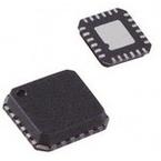
●This device is available in a 24-pin LFCSP package. It is specified for operation over the standard industrial temperature range of −40°C to +85°C.
●Applications
● Low jitter clock distribution
● Clock and data signal restoration
● Level translation
● Wireless communications
● Wired communications
● Medical and industrial imaging
● ATE and high performance instrumentation
●### Features and Benefits
● Selectable LVDS/CMOS outputs
● Up to 6 LVDS (1.2 GHz) or 12 CMOS (250 MHz) outputs
● <16 mW per channel (100 MHz operation)
● 54 fs integrated jitter (12 kHz to 20 MHz)
● 100 fs additive broadband jitter
● 2.0 ns propagation delay (LVDS)
● 135 ps output rise/fall (LVDS)
● 65 ps output-to-output skew (LVDS)
● Sleep mode
● Pin-programmable control
● 1.8 V power supply


