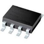
| TYPE | DESCRIPTION |
|---|
| Mounting Style | Surface Mount |
| Frequency | 7.5 GHz |
| Number of Pins | 16 Pin |
| Supply Voltage (DC) | 2.97V (min) |
| Case/Package | LFCSP-16 |
| Number of Outputs | 1 Output |
| Number of Circuits | 1 Circuit |
| Number of Positions | 16 Position |
| Operating Temperature (Max) | 125 ℃ |
| Operating Temperature (Min) | -40 ℃ |
| Supply Voltage | 2.97V ~ 3.63V |
| Supply Voltage (Max) | 3.63 V |
| Supply Voltage (Min) | 2.97 V |
| TYPE | DESCRIPTION |
|---|
| Product Lifecycle Status | Active |
| Packaging | Tape & Reel (TR) |
| Size-Width | 3 mm |
| Size-Height | 0.83 mm |
| Operating Temperature | -40℃ ~ 125℃ |
The ADCLK914BCPZ-R7 is an ultrafast SiGe open-collector HVDS Clock/Data Buffer feature high voltage differential signalling (HVDS) outputs. It is suitable for driving the latest Analog Devices high-speed digital-to-analogue converters (DACs). The ADCLK914 has a single, differential open-collector output. The ADCLK914 buffer operates up to 7.5GHz with a 160ps propagation delay and adds only 110fs random jitter (RJ). The input has a centre tapped, 100R, on-chip termination resistor and accepts LVPECL, CML, CMOS, LVTTL or LVDS (AC-coupled only). A VREF pin is available for biasing ac-coupled inputs. The HVDS output stage is designed to directly drive 1.9V each side into 50R terminated to VCC for a total differential output swing of 3.8V.
● On-chip input terminations
● 160ps Propagation delay
● 100ps Output rise/fall
● 110fs Random jitter
ADI
Ultrafast, SiGe, Open-Collector HVDS Clock/Data Buffer
ADI
Clock Buffer 1Out 1IN 1:1 16Pin LFCSP EP T/R
ADI
Clock Buffer 1Out 1IN 1:1 16Pin LFCSP EP T/R
ADI
Clock Buffer 1Out 1IN 1:1 16Pin LFCSP EP Tray
ADI
ANALOG DEVICES ADCLK914/PCBZ Evaluation Board, Clock & Timing, Clock Buffer, ADCLK914
Part Datasheet PDF Search
72,405,303 Parts Datasheet PDF, Update more than 5,000 PDF files ervery day.


