Product Details
●The ADL5501 is a mean-responding power detector for use in high frequency receiver and transmitter signal chains from 50 MHz to 6 GHz. It is easy to apply, requiring only a single supply between 2.7 V and 5.5 V and a power supply decoupling capacitor. The input is internally ac-coupled and has a nominal input impedance of 50 Ω. The output is a linear-responding dc voltage with a conversion gain of 6.3 V/V rms at 900 MHz.
●The ADL5501 is intended for true power measurement of simple and complex waveforms. The device is particularly useful for measuring high crest factor (high peak-to-rms ratio) signals, such as CDMA-, CDMA2000-, W-CDMA-, and QPSK-/QAM-based OFDM waveforms. The on-chip modulation filter provides adequate averaging for most waveforms.
●The on-chip, 100 Ω series resistance at the output, combined with an external shunt capacitor, creates a low-pass filter response that reduces the residual ripple in the dc output voltage. For more complex waveforms, an external capacitor at the FLTR pin can be used for supplementary signal demodulation.
●The ADL5501 offers excellent temperature stability across a 30 dB range and near 0 dB measurement error across temperature over the top portion of the dynamic range. In addition to its temperature stability, the ADL5501 offers low process variations that further reduce calibration complexity.
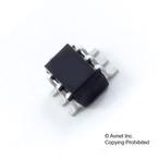
●The ADL5501 operates from −40°C to +85°C and is available in a small 6-lead SC-70 package. It is fabricated on a proprietary high fT silicon bipolar process.
●Applications
● Measurement of CDMA-, CDMA2000-, W-CDMA-, and QPSK-/ QAM-based OFDM, and other complex modulation
●waveforms
● RF transmitter or receiver power measurement
●### Features and Benefits
● True rms response
● Excellent temperature stability
● Up to 30 dB input dynamic range
● 50 Ω input impedance
● 1.25 V rms, 15 dBm, maximum input
● Single-supply operation: 2.7 V to 5.5 V
● Low power: 3.3 mW at 3 V supply
● RoHS-compliant


