GENERAL DESCRIPTION
●The ADSP-218xN series consists of six single chip microcomputers optimized for digital signal processing applica tions. The high-level block diagram for the ADSP-218xN series members appears on the previous page. All series members are pin-compatible and are differentiated solely by the amount of on-chip SRAM. This feature, combined with ADSP-21xx code compatibility, provides a great deal of flexibility in the design decision.
●PERFORMANCE FEATURES
●12.5 ns Instruction Cycle Time @1.8 V (Internal), 80 MIPS Sustained Performance
●Single-Cycle Instruction Execution
●Single-Cycle Context Switch
●3-Bus Architecture Allows Dual Operand Fetches in Every Instruction Cycle
●Multifunction Instructions
●Power-Down Mode Featuring Low CMOS Standby
● Power Dissipation with 200 CLKIN Cycle Recovery from Power-Down Condition
●Low Power Dissipation in Idle Mode
●INTEGRATION FEATURES
●ADSP-2100 Family Code Compatible (Easy to Use Algebraic Syntax), with Instruction Set Extensions
●Up to 256K Bytes of On-Chip RAM, Configured as
● Up to 48K Words Program Memory RAM
● Up to 56K Words Data Memory RAM
●Dual-Purpose Program Memory for Both Instruction and Data Storage
●Independent ALU, Multiplier/Accumulator, and Barrel Shifter Computational Units
●Two Independent Data Address Generators
●Powerful Program Sequencer Provides Zero Overhead Looping Conditional Instruction Execution
●Programmable 16-Bit Interval Timer with Prescaler
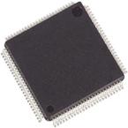
●100-Lead LQFP and 144-Ball Mini-BGA


