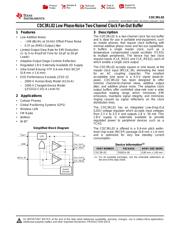
The CDC3RL02 is a two-channel clock fan-out buffer and is ideal for use in portable end-equipment, such as mobile phones, that require clock buffering with minimal additive phase noise and fan-out capabilities. It buffers a single master clock, such as a temperature compensated crystal oscillator (TCXO) to multiple peripherals. The device has two clock request inputs (CLK_REQ1 and CLK_REQ2), each of which enable a single clock output.
●The CDC3RL02 accepts square or sine waves at the master clock input (MCLK_IN), eliminating the need for an AC coupling capacitor. The smallest acceptable sine wave is a 0.3-V signal (peak-to-peak). CDC3RL02 has been designed to offer minimal channel-to-channel skew, additive output jitter, and additive phase noise. The adaptive clock output buffers offer controlled slew-rate over a wide capacitive loading range which minimizes EMI emissions, maintains signal integrity, and minimizes ringing caused by signal reflections on the clock distribution lines.
●The CDC3RL02 has an integrated Low-Drop-Out (LDO) voltage regulator which accepts input voltages from 2.3 V to 5.5 V and outputs 1.8 V, 50 mA. This 1.8-V supply is externally available to provide regulated power to peripheral devices such as a TCXO.
●The CDC3RL02 is offered in a 0.4-mm pitch wafer-level chip-scale (WCSP) package (0.8 mm × 1.6 mm) and is optimized for very low standby current consumption.
● Low Additive Noise:
● –149 dBc/Hz at 10-kHz Offset Phase Noise
● 0.37 ps (RMS) Output Jitter
● Limited Output Slew Rate for EMI Reduction
●(1- to 5-ns Rise/Fall Time for 10-pF to 50-pF
●Loads)
● Adaptive Output Stage Controls Reflection
● Regulated 1.8-V Externally Available I/O Supply
● Ultra-Small 8-bump YFP 0.4-mm Pitch WCSP
●(0.8 mm × 1.6 mm)
● ESD Performance Exceeds JESD 22
● 2000-V Human-Body Model (A114-A)
● 1000-V Charged-Device Model
●(JESD22-C101-A Level III)