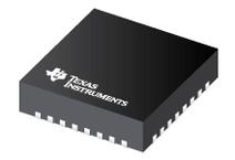
| TYPE | DESCRIPTION |
|---|
| Mounting Style | Surface Mount |
| Frequency | 1.1 GHz |
| Number of Pins | 32 Pin |
| Supply Voltage (DC) | 2.50 V |
| Case/Package | VQFN-32 |
| Number of Outputs | 10 Output |
| Number of Circuits | 1 Circuit |
| Number of Positions | 32 Position |
| Duty Cycle | 55 % |
| Maximum Duty Cycle | 55 % |
| Operating Temperature (Max) | 85 ℃ |
| Operating Temperature (Min) | -40 ℃ |
| Supply Voltage | 2.375V ~ 2.625V |
| Supply Voltage (Max) | 2.625 V |
| Supply Voltage (Min) | 2.375 V |
| TYPE | DESCRIPTION |
|---|
| Product Lifecycle Status | Active |
| Packaging | Tape & Reel (TR) |
| Size-Length | 5 mm |
| Size-Width | 5 mm |
| Size-Height | 0.9 mm |
| Operating Temperature | -40℃ ~ 85℃ |
The CDCLVD110ARHBT is a programmable low-voltage Clock Driver distributes one pair of differential LVDS clock inputs (either CLK0 or CLK1) to 10 pairs of differential clock outputs (Q0-Q9) with minimum skew for clock distribution. The CDCLVD110A is specifically designed to drive 50R transmission lines. When the control enable is high (EN=1), the 10 differential outputs are programmable in that each output can be individually enabled/disabled (3-stated) according to the first 10-bit loaded into the shift register. Once the shift register is loaded, the last bit selects either CLK0 or CLK1 as the clock input. However, when EN = 0, the outputs are not programmable and all outputs are enabled. The CDCLVD110A has an improved start-up circuit that minimizes enabling time in AC- and DC-coupled systems.
● <30ps Typical low-output skew for clock-distribution
● Distributes one differential clock input to ten LVDS differential clock outputs
● 2.5V at ±5% VCC range
● Typical signalling rate capability of up to 1.1GHz
● Full rail-to-rail common-mode input range
● ±100mV Receiver input threshold
● Green product and no Sb/Br
TI
1-to-10 LVDS clock buffer up to 900MHz with minimum skew for clock distributionN
TI
1-to-10 LVDS Clock Buffer up to 1100MHz with Minimum Skew for Clock Distribution 32-VQFN -40℃ to 85℃
TI
1-to-10 LVDS Clock Buffer up to 1100MHz with Minimum Skew for Clock Distribution 32-LQFP -40℃ to 85℃
TI
1-to-10 LVDS clock buffer up to 900MHz with minimum skew for clock distribution 32-LQFP -40℃ to 85℃
TI
1-to-10 LVDS Clock Buffer up to 1100MHz with Minimum Skew for Clock Distribution 32-LQFP -40℃ to 85℃
TI
1-to-10 LVDS clock buffer up to 900MHz with minimum skew for clock distribution 32-LQFP -40℃ to 85℃
TI
1-to-10 LVDS Clock Buffer up to 1100MHz with Minimum Skew for Clock Distribution 32-VQFN -40℃ to 85℃
TI
1-to-10 LVDS Clock Buffer up to 1100MHz with Minimum Skew for Clock Distribution 32-VQFN -40℃ to 85℃
TI
1-to-10 LVDS clock buffer up to 900MHz with minimum skew for clock distribution 32-LQFP -40℃ to 85℃
TI
1-to-10 LVDS Clock Buffer up to 1100MHz with Minimum Skew for Clock Distribution 32-VQFN -40℃ to 85℃
Part Datasheet PDF Search
72,405,303 Parts Datasheet PDF, Update more than 5,000 PDF files ervery day.


