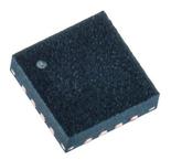
The CDCLVP1102RGTT is a highly versatile low additive Jitter Buffer can generate two copies of LVPECL clock outputs from one LVPECL, LVDS or LVCMOS input for a variety of communication applications. It has a maximum clock frequency up to 2GHz. The overall additive jitter performance is less than 0.1ps, RMS from 10kHz to 20MHz and overall output skew is as low as 10ps, making the device a perfect choice for use in demanding applications. The CDCLVP1102 clock buffer distributes a single clock input (IN) to two pairs of differential LVPECL clock outputs (OUT0, OUT1) with minimum skew for clock distribution. The inputs can be LVPECL, LVDS or LVCMOS/LVTTL. The CDCLVP1102 is specifically designed for driving 50R transmission lines. When driving the inputs in single-ended mode, the LVPECL bias voltage (VAC_REF) should be applied to the unused negative input pin. However, for high-speed performance up to 2GHz, differential mode is strongly recommended.
● 1:2 Differential buffer
● Single clock input
● Universal Inputs can accept LVPECL, LVDS and LVCMOS/LVTTL
● Two LVPECL outputs
● 2GHz Maximum clock frequency
● 33mA Maximum core current consumption
● <100fs Very low additive jitter
● 10ps Maximum output skew
● Green product and no Sb/Br
●Device has limited built-in ESD protection. The leads should be shorted together or the device placed in conductive foam during storage or handling to prevent electrostatic damage to the MOS gates.


