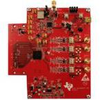
The DAC34SH84EVM is a circuit board that allows designers to evaluate the performance of Texas Instruments" four-channel, ultra-low power, 16-bit, 1.5 GSPS DAC34SH84 digital-to-analog converter (DAC) with 32-bit wide DDR LVDS data input, integrated 2x/4x/8x/16x interpolation filters, 32-bit NCO and PLL, and exceptional linearity at high IFs. The EVM provides a flexible environment to test the DAC34SH84 under a variety of clock, data input, and IF output conditions. For ease of use as a complete IF transmitter solution, the DAC34SH84EVM includes the Texas Instruments CDCE62005 clock generator/jitter cleaner for clocking the DAC34SH84. Besides providing a high-quality, low jitter DAC sampling clock to the DAC34SH84, the CDCE62005 also provides FPGA clocks to the TSW1400EVM (or TSW3100EVM) as FPGA reference clocks.
●The EVM can be used along with TSW1400 (or TSW3100) to perform a wide range of tests and measurements. The TSW1400 (or TSW3100) generates the test patterns which are fed to the DAC34SH84 through a 1.5 GSPS
● LVDS port. The on-board CDCE62005 can be used to synchronize the TSW1400 (or TSW3100) board to DAC34SH84EVM.
●The DAC34SH84EVM is also compatible with Xilinx and Altera based FPGA EVMs and design kits for rapid evaluation and prototyping. The DAC34SH84EVM includes an HSMC input for direct connection to HSMC compatible Altera based FPGA EVMs. The FMC-DAC-ADAPTER board available from TI enables the connection of the DAC34SH84EVM to the FMC header on Xilinx based EVMs.


