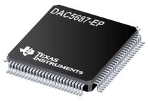
The DAC5687 is a dualchannel 16bit highspeed digitaltoanalog converter (DAC) with integrated 2×, 4×, and 8× interpolation filters, a complex numerically controlled oscillator (NCO), onboard clock multiplier, IQ compensation, and onchip voltage reference. The DAC5687 is pin compatible to the DAC5686, requiring only changes in register settings for most applications, and offers additional features and superior linearity, noise, crosstalk, and phase-locked loop (PLL) noise performance.
●The DAC5687 has six signal processing blocks: two interpolate by two digital filters, a finefrequency mixer with 32bit NCO, a quadrature modulation compensation block, another interpolate by two digital filter, and a coarsefrequency mixer with Fs/2 or Fs/4. The different modes of operation enable or bypass the signal processing blocks.
●The coarse and fine mixers can be combined to span a wider range of frequencies with fine resolution. The DAC5687 allows both complex or real output. Combining the frequency upconversion and complex output produces a Hilbert Transform pair that is output from the two DACs. An external RF quadrature modulator then performs the final single sideband upconversion.
●The IQ compensation feature allows optimization of phase, gain, and offset to maximize sideband rejection and minimize LO feedthrough for an analog quadrature modulator.
●The DAC5687 includes several input options: singleport interleaved data, even and odd multiplexing at half rate, and an input FIFO with either external or internal clock to ease the input timing ambiguity when the DAC5687 is clocked at the DAC output sample rate.
● Controlled Baseline
● One Assembly
● One Test Site
● One Fabrication Site
● Extended Temperature Performance of 55°C to 125°C
● Enhanced Diminishing Manufacturing Sources (DMS) Support
● Enhanced ProductChange Notification
● Qualification Pedigree(1)
● 500 MSPS
● Selectable 2×8× Interpolation
● OnChip PLL/VCO Clock Multiplier
● Full IQ Compensation Including Offset, Gain, and Phase
● Flexible Input Options
● FIFO With Latch on External or Internal Clock
● Even/Odd Multiplexed Input
● SinglePort Demultiplexed Input
● Complex Mixer With 32Bit Numerically Controlled Oscillator (NCO)
● FixedFrequency Mixer With Fs/4 and Fs/2
● 1.8V or 3.3V I/O Voltage
● OnChip 1.2V Reference
● Differential Scalable Output: 2 mA to 20 mA
● Pin Compatible to DAC5686
● High Performance
● 81dBc Adjacent Channel Leakage Ratio (ACLR) WCDMA TM1 at 30.72 MHz
● 72dBc ACLR WCDMA TM1 at 153.6 MHz
● Package: 100Pin HTQFP
● APPLICATIONS
● Cellular Base Transceiver Station Transmit Channel
● CDMA: WCDMA, CDMA2000, TDSCDMA
● TDMA: GSM, IS136, EDGE/UWC136
● OFDM: 802.16
● Cable Modem Termination System
●(1)Component qualification in accordance with JEDEC and industry standards to ensure reliable operation over an extended temperature range. This includes, but is not limited to, Highly Accelerated Stress Test (HAST) or biased 85/85, temperature cycle, autoclave or unbiased HAST, electromigration, bond intermetallic life, and mold compound life. Such qualification testing should not be viewed as justifying use of this component beyond specified performance and environmental limits.


