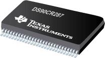
The DS90CR287 transmitter converts 28 bits of LVCMOS/LVTTL data into four LVDS (Low Voltage Differential Signaling) data streams. A phase-locked transmit clock is transmitted in parallel with the data streams over a fifth LVDS link. Every cycle of the transmit clock 28 bits of input data are sampled and transmitted.
●The DS90CR288A receiver converts the four LVDS data streams back into 28 bits of LVCMOS/LVTTL data. At a transmit clock frequency of 85 MHz, 28 bits of TTL data are transmitted at a rate of 595 Mbps per LVDS data channel. Using a 85 MHz clock, the data throughput is 2.38 Gbit/s (297.5 Mbytes/sec).
●This chipset is an ideal means to solve EMI and cable size problems associated with wide, high-speed TTL interfaces.
● 20 to 85 MHz Shift Clock Support
● 50% Duty Cycle on Receiver Output Clock
● 2.5 / 0 ns Set & Hold Times on TxINPUTs
● Low Power Consumption
● ±1V Common-Mode Range (around +1.2V)
● Narrow Bus Reduces Cable Size and Cost
● Up to 2.38 Gbps Throughput
● Up to 297.5 Mbytes/sec Bandwidth
● 345 mV (typ) Swing LVDS Devices for Low EMI
● PLL Requires no External Components
● Rising Edge Data Strobe
● Compatible with TIA/EIA-644 LVDS Standard
● Low Profile 56-Lead TSSOP Package


