DESCRIPTION
●The HCC4093B (extended temperature range) and HCF4093B(intermediate temperature range) are
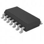
●available in 14-lead dual in-line plastic or ceramic package and plastic micropackage. The HCC/HCF4093Bconsists of four Schmitt-trigger circuits. Each circuit functions as a two-input NAND
●gate with Schmitt-trigger action on both inputs. The gate switches at different points for positive and negative-going signals. The difference between the positive voltage (VP) and the negative voltage (VN) is defined as hysteresis voltage (VH) (see fig. 1).
●.SCHMITT-TRIGGER ACTION ONEACH INPUT WITH NO EXTERNAL COMPONENTS
●.HYSTERESIS VOLTAGE TYPICALLY 0.9V AT VDD= 5V AND 2.3V AT VDD= 10V
●.NOISE IMMUNITY GREATER THAN 50% OF VDD(typ.)
●.NO LIMIT ON INPUT RISE AND FALL TIMES
●.STANDARDIZED SYMMETRICAL OUTPUT CHARACTERISTICS
●.QUIESCENT CURRENT SPECIFIED TO 20V FOR HCC DEVICE
●.5V, 10V, AND 15V PARAMETRIC RATINGS
●.INPUT CURRENT OF 100nA AT 18V AND 25°C FOR HCC DEVICE
●.100% TESTED FOR QUIESCENT CURRENT
●.MEETS ALL REQUIREMENTS OF JEDECTEN TATIVE STANDARD N°. 13A, ”STANDARD SPECIFICATIONS FOR DESCRIPTION OF ”B” SERIES CMOS DEVICES”


