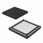
The MAX19516ETM+ is a dual channel, 10bit analogue to digital converter (ADC) in 48 pin TQFN package. It has maximum sample rate of 100Msps. The MAX19516 analogue input accepts wide 0.4V to 1.4V input common mode voltage range allowing DC coupled inputs for a wide range of RF, IF and baseband front end components. It provides excellent dynamic performance from baseband to high input frequencies beyond 400MHz making the device ideal for zero intermediate frequency (ZIF) and high intermediate frequency (IF) sampling applications. The typical signal to noise ratio (SNR) performance is 60dBFS and typical spurious free dynamic range (SFDR) is 82dBc at fIN = 70MHz and fCLK = 100MHz. The digital output drivers operate on an independent supply voltage (OVDD) over 1.8V to 3.5V range. The analogue power consumption is only 57mW per channel at VAVDD = 1.8V. In addition to low operating power, the MAX19516 consumes only 1mW in power-down mode and 17mW in standby mode.
● Supply voltage range from 1.7V to 3.5V (VOVDD)
● Operating temperature range from -40°C to 85°C
● ±0.25LSB INL at fIN = 3MHz, ±0.2LSB DNL at fIN = 3MHz, ±0.1%FS offset error & ±0.3%FS gain error
● Very low power operation (57mW/channel at 100Msps)
● 1.8V or 2.5V to 3.3V analogue supply and very high analogue input bandwidth of > 850MHz
● Single ended or differential analogue inputs and single ended or differential clock input
● User programmable adjustments and feature selection through an SPI interface
● Selectable data bus (dual CMOS or single multiplexed CMOS) and data output test patterns
● Reversible bit order (programmable), CMOS output internal termination options (programmable)
● Maximum clock frequency of 100MHz and minimum clock frequency of 50MHz


