Overview
●The Kinetis K28 USB ARM Cortex-M4 MCUs target applications requiring processing efficiency and extra-large embedded memory with 2 MB Flash and 1 MB SRAM. This microcontroller sub-family is:
● Highly integrated with two I2S interfaces, two USB Controllers (High-Speed with integrated High-Speed PHY and Full-Speed) and mainstream analog peripherals
● Expandable through a 32-bit SDRAM memory controller and QuadSPI interface supporting eXecution-In-Place (XiP)
● Enabling secure content using a True Random Number Generator, Cyclic Redundancy Check, Memory Mapped Cryptographic Acceleration Unit
●3 Input supply voltage rails: (1.2V, 1.8V and 3V) + separate VBAT domain
●K28 implements a Power Management Controller supporting Core Voltage Bypass and can be powered by an external PMIC to maximize the power efficiency of the overall system
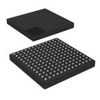
●Packages: 169 MAPBGA (9x9mm2, 0.65mm pitch) and 210 WLCSP (6.9x6.9mm2, 0.4 mm pitch)
●Evaluation / Development platform: FRDM-K28F
●MoreLess
●## Features
●### Performance
● 150 MHz (max) ARM Cortex-M4 with DSP instructions and Single Precision Floating Point unit (FPU)
● 32-channel DMA with asynchronous support in Stop mode
● Cross bar switch enables concurrent multi-master bus accesses, increasing bus bandwidth
●### Ultra-Low-Power
● Active run power core consumption @120Mhz: <258 µA/MH (TYP) (@25C) running from internal flash
● Static power consumption down to <14µA with full 1MB SRAM retention and <6 µS wakeup
● Lowest static mode down to 254 nA (VLLS0)
●### Memory
● 2 MB dual bank embedded program flash
● 1 MB of SRAM
● 8 KB I/D Cache + 8 KB System Cache
● 32-bit SDRAM controller
● QuadSPI interface with eXecution-In-Place (XiP)
●### Mixed-Signal Capability
● 16-bit SAR ADC: Up to 18ch Single-Ended / 3ch Differential
● 12-bit DAC
● Two analog comparators (CMP) containing a 6-bit DAC and programmable reference input
● 1.2V Analog voltage reference
●### Timing and Control
● One 4 ch-Periodic interrupt timer
● Two 16-bit low-power timer PWM modules
● Two 8-ch motor control/general purpose/PWM timers
● Two 2-ch quadrature decoder/general purpose timers
● Real-time clock with independent 3.6 V power domain
● Programmable delay block
●### Human-Machine Interface (HMI)
● 32-ch Programmable module (FlexIO) to emulate various serial, parallel or custom interfaces
●### Connectivity and Communications
● Dual USB Controllers: High-Speed (HS) w/ integrated HS PHY + crystal-less Full-Speed (FS) operations
● Five Low Power UART (LPUART) modules
● Two I2S modules for audio system interfacing and four I2C modules
● Four SPI modules (One supports up to 40 Mbps)
● Secure Digital Host Controller (SDHC)
●### Reliability, Safety and Security
● Cyclic redundancy check (CRC) engine validates memory contents and communication data, increasing system reliability
● True random number generator (TRNG)
● Memory Mapped Crypto Acceleration Unit (MMCAU): 256-bit DES, AES, SHA acceleratorComparison Table
●Kinetis MCU sub-family | Flash | SRAM | PMC w/ Core Voltage Bypass | Packages | Development board
●\---|---|---|---|---|---
●K28 | 2 MB | 1 MB | Yes | 210 WLCSP
●169 MAPBGA | FRDM-K28F
●K27 | 2 MB | 1 MB | No | 169 MABPGA | FRDM-K28F


