Part Datasheet Search > Interface ICs > NXP > PCA9509DP,118 Datasheet PDF
PCA9509DP,118 Datasheet PDF - NXP
| Manufacturer: | NXP |
| Category: | Interface ICs |
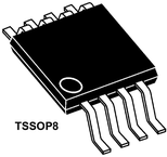
| Case Package: | TSSOP-8 |
| Description: | I²C Logic Repeater 3.3V/5V 8Pin TSSOP T/R |
| Documentation: | PCA9509DP,118 Datasheet (158 Pages)PCA9509DP,118 User Reference Manual Guide (64 Pages)PCA9509DP,118 Application Note (11 Pages) |
| Pictures: |
PCA9509DP,118 Datasheet PDF
ADatasheet has not yet included the datasheet for PCA9509DP,118
If necessary, please send a supplementary document request to the administrator

PCA9509DP,118 Datasheet PDF (158 Pages)
PCA9509DP,118 Specifications
| TYPE | DESCRIPTION |
|---|---|
| Mounting Style | Surface Mount |
| Number of Pins | 8 Pin |
| Supply Voltage (DC) | 3.00V (min) |
| Case/Package | TSSOP-8 |
| Supply Current | 3 mA |
| Number of Channels | 2 Channel |
| Number of Positions | 8 Position |
| Power Dissipation | 100 mW |
| Input Capacitance | 2 pF |
| Operating Temperature (Max) | 85 ℃ |
| Operating Temperature (Min) | -40 ℃ |
| Power Dissipation (Max) | 100 mW |
| Supply Voltage | 3V ~ 5.5V |
| Supply Voltage (Max) | 5.5 V |
| Supply Voltage (Min) | 3 V |
PCA9509DP,118 Size & Package
| TYPE | DESCRIPTION |
|---|---|
| Product Lifecycle Status | Active |
| Packaging | Tape & Reel (TR) |
| Size-Length | 3.1 mm |
| Size-Width | 3.1 mm |
| Size-Height | 0.95 mm |
| Operating Temperature | -40℃ ~ 85℃ |
PCA9509DP,118 Environmental
PCA9509DP,118 Export Classifications
PCA9509DP,118 Function Overview
Overview
●The PCA9509 is a level translating I²C-bus/SMBus repeater that enables processor low voltage 2-wire serial bus to interface with standard I²C-bus or SMBus I/O. While retaining all the operating modes and features of the I²C-bus system during the level shifts, it also permits extension of the I²C-bus by providing bidirectional buffering for both the data (SDA) and the clock (SCL) lines, thus enabling the I²C-bus or SMBus maximum capacitance of 400 pF on the higher voltage side. Port A allows a voltage range from 1.35 V to VCC(B) ‑ 1.0 V and requires no external pull-up resistors due to the internal current source. Port B allows a voltage range from 3.0 V to 5.5 V and is overvoltage tolerant. Both port A and port B SDA and SCL pins are high-impedance when the PCA9509 is unpowered.
●For applications where Port A VCC(A) is less than 1.35 V or Port B VCC(B) is less than 3.0 V, use drop-in replacement PCA9509A.
●The bus port B drivers are compliant with SMBus I/O levels, while port A uses a current sensing mechanism to detect the input or output LOW signal which prevents bus lock-up. Port A uses a 1 mA current source for pull-up and a 200 Ω pull-down driver. This results in a LOW on the port A accommodating smaller voltage swings. The output pull-down on the port A internal buffer LOW is set for approximately 0.2 V, while the input threshold of the internal buffer is set about 50 mV lower than that of the output voltage LOW. When the port A I/O is driven LOW internally, the LOW is not recognized as a LOW by the input. This prevents a lock-up condition from occurring. The output pull-down on the port B drives a hard LOW and the input level is set at 0.3 of SMBus or I²C-bus voltage level which enables port B to connect to any other I²C-bus devices or buffer.
●The PCA9509 drivers are not enabled unless VCC(A) is above 0.8 V and VCC(B) is above 2.5 V. The enable (EN) pin can also be used to turn on and turn off the drivers under system control. Caution should be observed to change only the state of the EN pin when the bus is idle.
●MoreLess
●## Features
● Bidirectional buffer isolates capacitance and allows 400 pF on port B of the device
● Voltage level translation from port A (1.35 V to VCC(B) ‑ 1.0 V) to port B (3.0 V to 5.5 V)
● Requires no external pull-up resistors on lower voltage port A
● Active HIGH repeater enable input
● Open-drain inputs/outputs
● Lock-up free operation
● Supports arbitration and clock stretching across the repeater
● Accommodates Standard-mode and Fast-mode I²C-bus devices and multiple masters
● Powered-off high-impedance I²C-bus pins
● Operating supply voltage range of 1.35 V to VCC(B) ‑ 1.0 V on port A, 3.0 V to 5.5 V on port B
● 5 V tolerant port B SCL, SDA and enable pins
● 0 Hz to 400 kHz clock frequency
●Remark
●: The maximum system operating frequency may be less than 400 kHz because of the delays added by the repeater.
● ESD protection exceeds 2000 V HBM per JESD22-A114 and 1000 V CDM per JESD22-C101
● Latch-up testing is done to JEDEC Standard JESD78 which exceeds 100 mA
● Packages offered: TSSOP8, SO8, XQFN8
●## Features
show more
PCA9509DP,118 Documents
PCA9509 Documents
Part Datasheet PDF Search
Example: STM32F103
72,405,303 Parts Datasheet PDF, Update more than 5,000 PDF files ervery day.

