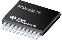
The PCM510xA devices are a family of monolithic CMOS-integrated circuits that include a stereo digital-to-analog converter and additional support circuitry in a small TSSOP package. The PCM510xA devices use the latest generation of TIs advanced segment-DAC architecture to achieve excellent dynamic performance and improved tolerance to clock jitter.
●Using Directpath™ charge-pump technology, the PCM510xA devices provide 2.1-VRMS ground centered outputs, allowing designers to eliminate DC blocking capacitors on the output, as well as external muting circuits traditionally associated with single-supply line drivers.
●The integrated line driver surpasses all other charge-pump based line drivers by supporting loads down to 1 kΩ per pin.
●The integrated PLL on the device removes the requirement for a system clock (commonly known as master clock), allowing a 3-wire I2S connection and reducing system EMI.
●Intelligent clock error and PowerSense undervoltage protection utilizes a two-level mute system for pop-free performance.
●Compared with many conventional switched capacitor DAC architectures, the PCM510xA family offers up to 20 dB lower out-of-band noise, reducing EMI and aliasing in downstream amplifiers/ADCs, measured from the traditional 100-kHz OBN measurements to 3 MHz).
● Ultra Low Out-of-Band Noise
● Integrated High-Performance Audio PLL with BCK
●Reference to Generate SCK Internally
● Direct Line Level 2.1-VRMS Output
● No DC Blocking Capacitors Required
● Line Level Output Down to 1KΩ
● Intelligent Muting System; Soft Up or Down Ramp
●and Analog Mute For 120-dB Mute SNR
● Accepts 16-, 24-, and 32-Bit Audio Data
● PCM Data Formats: I2S, Left-Justified
● Automatic Power-Save Mode When LRCK And
●BCK Are Deactivated
● 1.8 V or 3.3 V Failsafe LVCMOS Digital Inputs
● Simple Configuration Using Hardware Pins
● Single-Supply Operation: 14
● 3.3 V Analog, 1.8 V or 3.3 V Digital
● Qualified in Accordance with AEC-Q100


