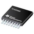
The SN65LVDM050PW is a differential Line Driver and Receiver uses low-voltage differential signaling (LVDS) to achieve high signaling rates. This circuit is similar to TIA/EIA-644 standard compliant devices (SN65LVDS) counterparts, except that the output current of the drivers is doubled. This modification provides a minimum differential output voltage magnitude of 247mV across a 50R load simulating two transmission lines in parallel. This allows having data buses with more than one driver or with two line termination resistors. The receiver detects a voltage difference of 50mV with up to 1V of ground potential difference between a transmitter and receiver. The intended application of this device and signaling technique is point-to-point half duplex, baseband data transmission over a controlled impedance media of approximately 100R characteristic impedance. The transmission media may be printed-circuit board traces, backplanes or cables.
● Typical full-duplex signalling rate of 100Mbps
● Bus-terminal ESD exceeds 12kV
● Low-voltage differential signaling with typical output voltage of 340mV with a 50R load
● Valid output with as little as 50mV input voltage difference
● Propagation delay time - 1.7ns Typical driver and 3.7ns typical receiver
● Power dissipation at 200MHz - 50mW Typical driver and 60mW typical receiver
● LVTTL input levels are 5V tolerant
● Driver is high-impedance when disabled or with VCC <1.5V
● Receiver has open-circuit failsafe design
● Green product and no Sb/Br


