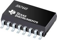
These monolithic BCD-to-decimal decoders/drivers consist of eight inverters and ten four-input NAND gates. The inverters are connected in pairs to make BCD input data available for decoding by the NAND gates. Full decoding of valid BCD input logic ensures that all outputs remain off for all invalid binary input conditions. These decoders feature TTL inputs and high-performance, n-p-n output transistors designed for use as indicator/relay drivers or as open-collector logic-circuit drivers. Each of the high-breakdown output transistors (30 volts) will sink up to 80 milliamperes of current. Each input is one normalized Series 54 /74 load. Inputs and outputs are entirely compatible for use with TTL logic circuits, and the outputs are compatible for interfacing with most MOS integrated circuits. Power dissipation is typically 215 milliwatts.
●## FOR USE AS LAMP, RELAY, OR MOS DRIVERS
●## featuring
● Full Decoding of Input Logic
● 80-mA Sink-Current Capability
● All Outputs Are Off for Invalid BCD Input Conditions
Part Datasheet PDF Search
72,405,303 Parts Datasheet PDF, Update more than 5,000 PDF files ervery day.


