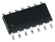
The SN74LVC125ADR is a Quadruple Bus Buffer Gate, designed for 1.65 to 3.6V VCC operation. The SN74LVC125ADR device features independent line drivers with 3-state outputs. Each output is disabled when the associated output-enable (OE) input is high. To ensure the high-impedance state during power up or power down, OE should be tied to VCC through a pull-up resistor, the minimum value of the resistor is determined by the current-sinking capability of the driver. Inputs can be driven from either 3.3 or 5V devices. This feature allows the use of this device as a translator in a mixed 3.3/5V system environment. ESD protection exceeds JESD 22, 2000V human-body model, 200V machine model and 1000V charged-device model.
● 3-state Outputs
● Separate OE for all 4 buffers
● Inputs accept voltages to 5.5V
● Maximum TPD of 4.8ns at 3.3V
● <0.8V at VCC = 3.3V, TA = 25°C Typical VOLP (output ground bounce)
● >2V at VCC = 3.3V, TA = 25°C Typical VOHV (output VOH undershoot)
● Latch-up performance exceeds 250mA per JESD 17
● Green product and no Sb/Br
●Device has limited built-in ESD protection. The leads should be shorted together or the device placed in conductive foam during storage or handling to prevent electrostatic damage to the MOS gates.


