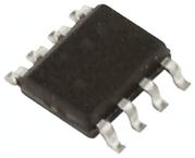
The SN74LVC2G125DCUR is a dual Bus Buffer Gate designed for 1.65 to 5.5V VCC operation. This device features dual line drivers with 3-state outputs. The outputs are disabled when the associated output-enable (OE) input is high. To ensure the high-impedance state during power up or power down, OE should be tied to VCC through a pull-up resistor and the minimum value of the resistor is determined by the current-sinking capability of the driver. This device is fully specified for partial-power-down applications using IOFF. The IOFF circuitry disables the outputs, preventing damaging current backflow through the device when it is powered down. This device contains dual buffer gate device with output enable control and performs the Boolean function Y = A. To ensure the high-impedance state during power up or power down, OE should be tied to VCC through a pull-up resistor and the minimum value of the resistor is determined by the current-sinking capability of the driver.
● IOFF Supports live insertion, partial-power-down mode and back-drive protection
● Allows down voltage translation
● Can be used as a down translator to translate inputs from 5.5V down to the VCC level
● Inputs accept voltages to 5.5V
● Latch-up performance exceeds 250mA per JESD 17
● 4.3ns at 3.3V Propagation delay (tpd)
● 10µA ICC Low power consumption
● ±24mA Output drive at 3.3 V
● <0.8V at VCC = 3.3V, TA = 25°C VOLP (output ground bounce)
● >2V at VCC = 3.3V, TA = 25°C VOHV (output VOH undershoot)
● Green product and no Sb/Br


