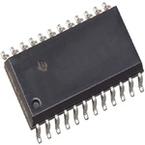
The SN74LVC827ADW is a 10-bit Buffer/Bus Driver designed for 1.65 to 3.6V VCC operation. It provides a high-performance bus interface for wide data paths or buses carrying parity. The 3-state control gate is a 2-input AND gate with active-low inputs so that, if either output-enable (OE1 or OE2) input is high, all ten outputs are in the high-impedance state. It provides true data at its outputs. Inputs can be driven from either 3.3/5V devices. This feature allows the use of this device as a translator in a mixed 3.3/5V system environment. To ensure the high-impedance state during power up or power down, OE should be tied to VCC through a pull-up resistor and the minimum value of the resistor is determined by the current-sinking capability of the driver. This device is fully specified for partial-power-down applications using IOFF. The IOFF circuitry disables the outputs, preventing damaging current backflow through the device when it is powered down.
● Support mixed-mode signal operation on all ports
● Allows down voltage translation
● IOFF Supports live insertion, partial-power-down mode and back-drive protection
● Latch-up performance exceeds 250mA per JESD 17
● Inputs accept voltages to 5.5V
● 6.7ns at 3.3V Propagation delay (tpd)
● <0.8V at VCC = 3.3V, TA = 25°C VOLP (output ground bounce)
● >2V at VCC = 3.3V, TA = 25°C VOHV (output VOH undershoot)
● Green product and no Sb/Br


