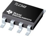
The TLC548 and TLC549 are CMOS analog-to-digital converter (ADC) integrated circuits built around an 8-bit switched-capacitor successive-approximation ADC. These devices are designed for serial interface with a microprocessor or peripheral through a 3-state data output and an analog input. The TLC548 and TLC549 use only the input/output clock (I/O CLOCK) input along with the chip select (CS\\) input for data control. The maximum I/O CLOCK input frequency of the TLC548 is 2.048 MHz, and the I/O CLOCK input frequency of the TLC549 is specified up to 1.1 MHz.
●Operation of the TLC548 and the TLC549 is very similar to that of the more complex TLC540 and TLC541 devices; however, the TLC548 and TLC549 provide an on-chip system clock that operates typically at 4 MHz and requires no external components. The on-chip system clock allows internal device operation to proceed independently of serial input/output data timing and permits manipulation of the TLC548 and TLC549 as desired for a wide range of software and hardware requirements. The I/O CLOCK together with the internal system clock allow high-speed data transfer and conversion rates of 45 500 conversions per second for the TLC548, and 40 000 conversions per second for the TLC549.
●Additional TLC548 and TLC549 features include versatile control logic, an on-chip sample-and-hold circuit that can operate automatically or under microprocessor control, and a high-speed converter with differential high-impedance reference voltage inputs that ease ratiometric conversion, scaling, and circuit isolation from logic and supply noises. Design of the totally switched-capacitor successive-approximation converter circuit allows conversion with a maximum total error of ±0.5 least significant bit (LSB) in less than 17 us.
●The TLC548C and TLC549C are characterized for operation from 0°C to 70°C. The TLC548I and TLC549I are characterized for operation from -40°C to 85°C.
● Microprocessor Peripheral or Standalone Operation
● 8-Bit Resolution A/D Converter
● Differential Reference Input Voltages
● Conversion Time . . . 17 us Max
● Total Access and Conversion Cycles Per Second
●\- TLC548 . . . up to 45 500
●\- TLC549 . . . up to 40 000
● On-Chip Software-Controllable Sample-and-Hold Function
● Total Unadjusted Error . . . ±0.5 LSB Max
● 4-MHz Typical Internal System Clock
● Wide Supply Range . . . 3 V to 6 V
● Low Power Consumption . . . 15 mW Max
● Ideal for Cost-Effective, High-Performance Applications including Battery-Operated Portable Instrumentation
● Pinout and Control Signals Compatible With the TLC540 and TLC545 8-Bit A/D Converters and with the TLC1540 10-Bit A/D Converter
● CMOS Technology


