description
●This data sheet provides complete design documentation for the second-generation devices of the TMS320 family. This facilitates the selection of the devices best suited for user applications by providing all specifications and special features for each TMS320 member. This data sheet is divided into four major sections: architecture, electrical specifications (NMOS and CMOS), timing diagrams, and mechanical data. In each of these sections, generic information is presented first, followed by specific device information. An index is provided for quick reference to specific information about a device.
●• 80-ns Instruction Cycle Time
●• 544 Words of On-Chip Data RAM
●• 4K Words of On-Chip Secure Program EPROM (TMS320E25)
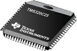
●• 4K Words of On-Chip Program ROM (TMS320C25)
●• 128K Words of Data/Program Space
●• 32-Bit ALU/Accumulator
●• 16 × 16-Bit Multiplier With a 32-Bit Product
●• Block Moves for Data/Program Management
●• Repeat Instructions for Efficient Use of Program Space
●• Serial Port for Direct Codec Interface
●• Synchronization Input for Synchronous Multiprocessor Configurations
●• Wait States for Communication to Slow Off-Chip Memories/Peripherals
●• On-Chip Timer for Control Operations
●• Single 5-V Supply
●• Packaging: 68-Pin PGA, PLCC, and CER-QUAD
●• 68-to-28 Pin Conversion Adapter Socket for EPROM Programming
●• Commercial and Military Versions Available
●• NMOS Technology:
●— TMS32020 . . . . . . . . . 200-ns cycle time
●• CMOS Technology:
●— TMS320C25 . . . . . . . . 100-ns cycle time
●— TMS320E25 . . . . . . . . 100-ns cycle time
●— TMS320C25-50 . . . . . . 80-ns cycle time


