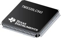
Part Datasheet Search > TI > TMS320LC543 Datasheet PDF
TMS320LC543 Datasheet PDF
ADatasheet has not yet included the datasheet for TMS320LC543
If necessary, please send a supplementary document request to the administrator

TMS320LC543 Datasheet PDF (118 Pages)
TMS320LC543 Environmental
TMS320LC543 Function Overview
The TMS320C54x, TMS320LC54x, and TMS320VC54x fixed-point, digital signal processor (DSP) families (hereafter referred to as the 54x unless otherwise specified) are based on an advanced modified Harvard architecture that has one program memory bus and three data memory buses. These processors also provide an arithmetic logic unit (ALU) that has a high degree of parallelism, application-specific hardware logic, on-chip memory, and additional on-chip peripherals. These DSP families also provide a highly specialized instruction set, which is the basis of the operational flexibility and speed of these DSPs.
●Separate program and data spaces allow simultaneous access to program instructions and data, providing the high degree of parallelism. Two reads and one write operation can be performed in a single cycle. Instructions with parallel store and application-specific instructions can fully utilize this architecture. In addition, data can be transferred between data and program spaces. Such parallelism supports a powerful set of arithmetic, logic, and bit-manipulation operations that can all be performed in a single machine cycle. In addition, the C54x, LC54x, and VC54x versions include the control mechanisms to manage interrupts, repeated operations, and function calls.
● Advanced Multibus Architecture With Three Separate 16-Bit Data Memory Buses and One Program Memory Bus
● 40-Bit Arithmetic Logic Unit (ALU) Including a 40-Bit Barrel Shifter and Two Independent 40-Bit Accumulators
● 17- × 17-Bit Parallel Multiplier Coupled to a 40-Bit Dedicated Adder for Non-Pipelined Single-Cycle Multiply/Accumulate (MAC) Operation
● Compare, Select, and Store Unit (CSSU) for the Add/Compare Selection of the Viterbi Operator
● Exponent Encoder to Compute an Exponent Value of a 40-Bit Accumulator Value in a Single Cycle
● Two Address Generators With Eight Auxiliary Registers and Two Auxiliary Register Arithmetic Units (ARAUs)
● Data Bus With a Bus Holder Feature
● Address Bus With a Bus Holder Feature (548 and 549 Only)
● Extended Addressing Mode for 8M × 16-Bit Maximum Addressable External Program Space (548 and 549 Only)
● 192K × 16-Bit Maximum Addressable Memory Space (64K Words Program, 64K Words Data, and 64K Words I/O)
● On-Chip ROM with Some Configurable to Program/Data Memory
● Dual-Access On-Chip RAM
● Single-Access On-Chip RAM (548/549)
● Single-Instruction Repeat and Block-Repeat Operations for Program Code
● Block-Memory-Move Instructions for Better Program and Data Management
● Instructions With a 32-Bit Long Word Operand
● Instructions With Two- or Three-Operand Reads
● Arithmetic Instructions With Parallel Store and Parallel Load
● Conditional Store Instructions
● Fast Return From Interrupt
● On-Chip Peripherals
● Software-Programmable Wait-State Generator and Programmable Bank Switching
● On-Chip Phase-Locked Loop (PLL) Clock Generator With Internal Oscillator or External Clock Source
● Full-Duplex Serial Port to Support 8- or 16-Bit Transfers (541, LC545, and LC546 Only)
● Time-Division Multiplexed (TDM) Serial Port (542, 543, 548, and 549 Only)
● Buffered Serial Port (BSP) (542, 543, LC545, LC546, 548, and 549 Only)
● 8-Bit Parallel Host-Port Interface (HPI) (542, LC545, 548, and 549)
● One 16-Bit Timer
● External-Input/Output (XIO) Off Control to Disable the External Data Bus, Address Bus and Control Signals
● Power Consumption Control With IDLE1, IDLE2, and IDLE3 Instructions With Power-Down Modes
● CLKOUT Off Control to Disable CLKOUT
● On-Chip Scan-Based Emulation Logic, IEEE Std 1149.1 (JTAG) Boundary Scan Logic
● 25-ns Single-Cycle Fixed-Point Instruction Execution Time [40 MIPS] for 5-V Power Supply (C541 and C542 Only)
● 20-ns and 25-ns Single-Cycle Fixed-Point Instruction Execution Time (50 MIPS and 40 MIPS) for 3.3-V PowerSupply (LC54x)
● 15-ns Single-Cycle Fixed-Point Instruction Execution Time (66 MIPS) for 3.3-V Power Supply (LC54xA, 548, LC549)
● 12.5-ns Single-Cycle Fixed-Point Instruction Execution Time (80 MIPS) for 3.3-V Power Supply (LC548, LC549)
● 10-ns and 8.3-ns Single-Cycle Fixed-Point Instruction Execution Time (100 and 120 MIPS) for 3.3-V Power Supply (2.5-V Core) (VC549)
●IEEE Standard 1149.1-1990 Standard-Test-Access Port and Boundary Scan Architecture.
show more
TMS320LC543 Documents
TMS320 Documents
TI
Digital Signal Processing (DSP) Fixed-Point 16Bit 40MHz 40MIPS 100Pin LQFP
TI
Digital Signal Processing (DSP) Fixed-Point 32Bit 100MHz 100MIPS 100Pin LQFP
Part Datasheet PDF Search
Example: STM32F103
72,405,303 Parts Datasheet PDF, Update more than 5,000 PDF files ervery day.
Relate Parts
Popular Parts
New Parts

