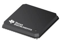
● High-Performance, Low-Power, Fixed-Point TMS320C55x™; Digital Signal Processor (DSP)
● 6.25-/5-ns Instruction Cycle Time
● 160-/200-MHz Clock Rate
● One/Two Instructions Executed per Cycle
● Dual Multipliers (Up to 400 Million Multiply-Accumulates Per Second (MMACS))
● Two Arithmetic/Logic Units
● One Internal Program Bus
● Three Internal Data/Operand Read Buses
● Two Internal Data/Operand Write Buses
● Instruction Cache (24K Bytes)
● 160K x 16-Bit On-Chip RAM Composed of:
● Eight Blocks of 4K × 16-Bit Dual-Access RAM (DARAM) (64K Bytes)
● 32 Blocks of 4K × 16-Bit Single-Access RAM (SARAM)(256K Bytes)
● 16K × 16-Bit On-Chip ROM (32K Bytes)
● 8M × 16-Bit Maximum Addressable External Memory Space
● 32-Bit External Memory Interface (EMIF) With Glueless Interface to:
● Asynchronous Static RAM (SRAM)
● Asynchronous EPROM
● Synchronous DRAM (SDRAM)
● Synchronous Burst SRAM (SBSRAM)
● Programmable Low-Power Control of Six Device Functional Domains
● On-Chip Peripherals
● Two 20-Bit Timers
● Six-Channel Direct Memory Access (DMA) Controller
● Three Multichannel Buffered Serial Ports (McBSPs)
● 16-Bit Parallel Enhanced Host-Port Interface (EHPI)
● Programmable Digital Phase-Locked Loop (DPLL) Clock Generator
● Eight General-Purpose I/O (GPIO) Pins and Dedicated General-Purpose Output (XF)
● On-Chip Scan-Based Emulation Logic
● IEEE Std 1149.1 (JTAG) Boundary Scan Logic
● 240-Terminal MicroStar BGA™; (Ball Grid Array) (GGW Suffix)
● 240-Terminal MicroStar BGA™; (Ball Grid Array) (ZGW Suffix) [Lead-Free]
● 3.3-V I/O Supply Voltage
● 1.6-V Core Supply Voltage


