
Part Datasheet Search > ADI > ADAU1452 Datasheet PDF > ADAU1452 Datasheet Pages 34/180

ADAU1452 Datasheet - ADI
| Manufacturer: | ADI |
| Description: | SigmaDSP Digital Audio Processor |
| Pictures: |
ADAU1452Datasheet PDF
Page:
of 180 Go
If the format of the manual is confusing, please download and read the original PDF file.
ADAU1452/ADAU1451/ADAU1450 Data Sheet
5
8
1
72
63
4
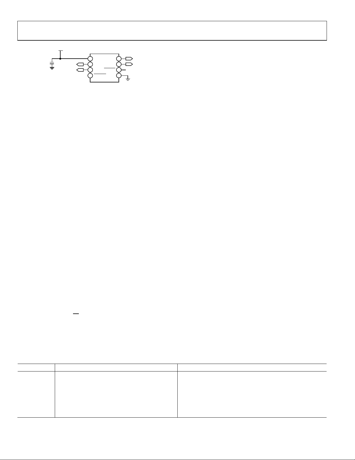
THERM
GND
ALERT
SDATA
VDD
D+
D–
SCLK
ADM1032
3.3V
SCL
SDA
100nF
THD_P
THD_M
11486-029
Figure 26. Example External Temperature Sensor Circuit
SLAVE CONTROL PORTS
A total of four control ports are available: two slave ports and two
master ports. The slave I2C port and slave SPI port allow an
external master device to modify the contents of the memory and
registers. The master I
2
C port and master SPI port allow the device
to self boot and to send control messages to slave devices on the
same bus.
Slave Control Port Overview
To program the DSP and configure the control registers, a slave
port is available that can communicate using either the I
2
C or SPI
protocols. A separate master communications port can be used
to self boot the chip by reading from an external EEPROM, or
to boot or control external ICs by addressing them directly using
I
2
C or SPI. The slave communications port defaults to I
2
C mode;
however, it can be put into SPI mode by toggling SS (SS/ADDR0),
the slave select pin, low three times. Each toggle should last
at least the duration of one clock period of the clock on MCLK
(XTALIN/MCLK), the master clock input pin. Until the PLL locks,
only the PLL configuration registers (Address 0xF000 to
Address 0xF004) are accessible. For this reason, always write to
the PLL registers first after the chip powers up. After the PLL
locks, the remaining registers and the RAM become accessible.
See the System Initialization Sequence section for more
information.
The control port is capable of full read/write operation for all
addressable registers. The ADAU1452/ADAU1451/ADAU1450
must have a valid master clock to write to all registers, with the
exception of Register 0xF000 to Register 0xF004. All addresses
can be accessed in both single address mode and burst mode.
The first byte (Byte 0) of a control port write contains the 7-bit
chip address plus the R/
W
bit. The next two bytes (Byte 1 and
Byte 2) together form the subaddress of the register location
within the memory maps of the ADAU1452/ADAU1451/
ADAU1450. This subaddress must be two bytes long because the
memory locations within the devices are directly addressable, and
their sizes exceed the range of single byte addressing. All subse-
quent bytes (starting with Byte 3) contain the data, such as control
port data, program data, or parameter data. The number of bytes
per word depends on the type of data that is being written.
The ADAU1452/ADAU1451/ADAU1450 have several mech-
anisms for updating signal processing parameters in real time
without causing pops or clicks.
If large blocks of data must be downloaded, halt the output of
the DSP core (using Register 0xF400, HIBERNATE), load new
data, and then restart the device (using Register 0xF402,
START_CORE). This process is typically performed during the
booting sequence at startup or when loading a new program
into RAM.
When updating a signal processing parameter while the DSP
core is running, use the software safeload function to avoid
a situation where a parameter is updated over the boundary of
an audio frame, which can lead to an audio artifact such as a
click or pop sound. For more information, see the Software
Safeload section.
The slave control port pins are multifunctional, depending on
the mode in which the device is operating. Table 30 describes
these multiple functions.
Burst Mode Writing and Reading
Burst write and read modes are available for convenience when
writing large amounts of data to contiguous registers. In these
modes, the chip and memory addresses are written once, and
then a large amount of data can follow uninterrupted. The sub-
addresses are automatically incremented at the word boundaries.
This increment happens automatically after a single word write
or read unless a stop condition is encountered (I
2
C mode) or the
slave select is disabled and brought high (SPI mode). A burst write
starts like a single word write, but, following the first data-word,
the data-word for the next address can be written immediately
without sending its 2-byte address. The control registers in the
ADAU1452/ADAU1451/ADAU1450 are two bytes wide, and the
memories are four bytes wide. The autoincrement feature
knows the word length at each subaddress; therefore, it is not
necessary to manually specify the subaddress for each address in a
burst write.
The subaddresses are automatically incremented by one address,
following each read or write of a data-word, regardless of whether
there is a valid register or RAM word at that address.
Table 30. Control Port Pin Functions
Pin Name
I
2
C Slave Mode
SPI Slave Mode
SS/ADDR0 Address 0 (Bit 1 of the address word, input to the
ADAU1452/ADAU1451/ADAU1450)
Slave select (input to the ADAU1452/ADAU1451/ADAU1450)
CCLK/SCL Clock (input to the ADAU1452/ADAU1451/ADAU1450) Clock (input to the ADAU1452/ADAU1451/ADAU1450)
MOSI/ADDR1 Address 1 (Bit 2 of the address word, input to the
ADAU1452/ADAU1451/ADAU1450)
Data; master out, slave in (input to the ADAU1452/ADAU1451/
ADAU1450)
MISO/SDA Data (bidirectional, open collector) Data; master in, slave out (output from the ADAU1452/ADAU1451/
ADAU1450)
Rev. C | Page 34 of 180