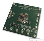
Part Datasheet Search > Development Kits > Linear Technology > DC1734A Datasheet PDF > DC1734A Datasheet Pages 1/36
DC1734ADatasheet PDF
Page:
of 36 Go
If the format of the manual is confusing, please download and read the original PDF file.

LT8582
1
8582f
TYPICAL APPLICATION
FEATURES DESCRIPTION
Dual 3A Boost/Inverting/SEPIC
DC/DC Converter with
Fault Protection
The LT
®
8582 is a dual independent channel PWM DC/DC
converter with a power good pin and built-in fault protection
to help guard against input overvoltage and overtempera-
ture conditions. Each channel consists of a 42V master
switch and a 42V slave switch that can be tied together
for a total current limit of 3A.
The LT8582 is ideal for many local power supply designs.
Each channel can be easily configured in boost, SEPIC,
inverting, or flyback configurations. Together, the two chan-
nels can produce a 12V and a –12V output with 14.4W of
combined output power from a 5V input. In addition, the
LT8582’s slave switch allows the part to be configured in
high voltage, high power charge pump topologies that
are more efficient and require fewer components than
traditional circuits.
The LT8582 also features innovative SHDN pin circuitry that
allows for slowly varying input signals and an adjustable
undervoltage lockout function. Additional features such as
output short protection, frequency foldback and soft-start
are integrated. The LT8582 is available in a 24-pin 7mm
× 4mm DFN package.
1.5MHz, 5V to ±12V
Efficiency and Power Loss
(Load Between 12V and –12V Outputs)
APPLICATIONS
n
Local Power Supply
n
Vacuum Fluorescent Display (VFD) Bias Supplies
n
TFT-LCD Bias Supplies
n
Automotive Engine Control Unit (ECU) Power
L, LT, LTC, LTM, Linear Technology and the Linear logo are registered trademarks and ThinSOT
is a trademark of Linear Technology Corporation. All other trademarks are the property of their
respective owners. Protected by U.S. Patents including 7579816.
n
Dual 42V, 3A Combined Power Switch
n
Master/Slave (1.7A/1.3A) Switch Design
n
Wide Input Range: 2.5V to 22V Operating, 40V
Maximum Transient
n
Power Good Pin for Event Based Sequencing
n
Switching Frequency Up to 2.5MHz
n
Each Channel Easily Configurable as a Boost, SEPIC,
Inverting or Flyback Converter
n
Low V
CESAT
Switch: 270mV at 2.75A (Typical)
n
Can be Synchronized to an External Clock
n
Output Short-Circuit Protection
n
High Gain SHDN Pin Accepts Slowly Varying Input
Signals
n
24-Pin 7mm × 4mm DFN Package
LOAD CURRENT (A)
0
20
EFFICIENCY (%)
POWER LOSS (W)
30
80
70
60
50
90
0.2
0.3 0.6
8582 TA01b
40
0.1
0.4
0.5
100
0
0.4
2.4
2.0
1.6
1.2
2.8
0.8
3.2
SWB2
SWA2
SWB1
SWA1
LT8582
8582 TA01a
PG1
SYNC1
CLKOUT1
CLKOUT2
215k
SYNC2
PG2
V
IN2
SHDN2
V
IN1
SHDN1
V
C1
SS1
RT1
GND
RT2
SS2
GATE2
V
C2
FBX2
FBX1
GATE1
V
OUT1
12V
550mA
V
OUT2
–12V
550mA
4.7µF
2.2µF
V
IN
5V
0.1µF
6.04k
0.1µF
53.6k
53.6k
4.7nF 47pF
47pF
14.7k
6.49k
100k
100k
143k
215k
4.7µH
s
4.7µH
s
2.2nF
10µF
10µF
130k
4.7µF 10µF
4.7µH
Part Datasheet PDF Search
72,405,303 Parts Datasheet PDF, Update more than 5,000 PDF files ervery day.

