GENERAL DESCRIPTION
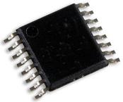
●The AD5306/AD5316/AD53261 are quad 8-/10-/12-bit buffered voltage output DACs in 16-lead TSSOP packages that operate from a single 2.5 V to 5.5 V supply, consuming 500 μA at 3 V. Their on-chip output amplifiers allow rail-to-rail output swing with a slew rate of 0.7 V/μs. A 2-wire serial interface, which operates at clock rates up to 400 kHz, is used. This interface is SMBus-compatible at VDD< 3.6 V. Multiple devices can be placed on the same bus.
●FEATURES
●AD5306: 4 buffered, 8-bit DACs in 16-lead TSSOP
●A version: ±1 LSB INL; B version: ±0.625 LSB INL
●AD5316: 4 buffered, 10-bit DACs in 16-lead TSSOP
●A version: ±4 LSB INL; B version: ±2.5 LSB INL
●AD5326: 4 buffered, 12-bit DACs in 16-lead TSSOP
●A version: ±16 LSB INL; B version: ±10 LSB INL
●Low power operation: 400 μA @ 3 V, 500 μA @ 5 V
●2-wire (I
●2
●C®-compatible) serial interface
●2.5 V to 5.5 V power supply
●Guaranteed monotonic by design over all codes
●Power-down to 90 nA @ 3 V, 300 nA @ 5 V (PDpin or bit)
●Double-buffered input logic
●Buffered/unbuffered reference input options
●Output range: 0 V to VREFor 0 V to 2 VREF
●Power-on reset to 0 V
●Simultaneous update of outputs (LDACpin)
●Software clear facility
●Data readback facility
●On-chip rail-to-rail output buffer amplifiers
●Temperature range −40°C to +105°C
●APPLICATIONS
●Portable battery-powered instruments
●Digital gain and offset adjustment
●Programmable voltage and current sources
●Programmable attenuators
●Industrial process control


