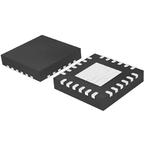
Product Details
●The AD7091R-2/AD7091R-4/AD7091R-8 family is a multichannel 12-bit, ultralow power, successive approximation analog-to-digital converter (ADC) that is available in two, four, or eight analog input channel options. The AD7091R-2/AD7091R-4/ AD7091R-8 operate from a single 2.7 V to 5.25 V power supply and are capable of achieving a sampling rate of 1 MSPS.
●The AD7091R-2/AD7091R-4/AD7091R-8 family offers up to eight single-ended analog input channels with a channel sequencer that allows a preprogrammed selection of channels to be converted sequentially. The AD7091R-2/AD7091R-4/ AD7091R-8 also feature an on-chip conversion clock, an on-chip accurate 2.5 V reference, and a high speed serial interface.
●The AD7091R-2/AD7091R-4/AD7091R-8 have a serial port interface (SPI) that allows data to be read after the conversion while achieving a 1 MSPS throughput rate. The conversion process and data acquisition are controlled using the CONVST pin.
●The AD7091R-2/AD7091R-4/AD7091R-8 use advanced design techniques to achieve ultralow power dissipation at high throughput rates. They also feature flexible power management options. An on-chip configuration register allows the user to set up different operating conditions. These include power management, alert functionality, busy indication, channel sequencing, and general-purpose output pins. The MUXOUT and ADCIN pins allow signal conditioning of the multiplexer output prior to acquisition by the ADC.
●Applications
● Battery powered systems
● Personal digital assistants
● Medical instruments
● Mobile communications
● Instrumentation and control systems
● Data acquisition systems
● Optical sensors
● Diagnostic/monitoring functions
●### Features and Benefits
● Ultralow system power
● Flexible power/throughput rate management
● Programmable ALERT interrupt pin
● High performance
● 1 MSPS throughput with no latency/pipeline delay
● SNR: 70 dB typical at 10 kHz input frequency
● THD: −80 dB typical at 10 kHz input frequency
● INL: ±0.7 LSB typical, ±1.0 LSB maximum
● Small system footprint
● On-chip accurate 2.5 V reference, 5 ppm/°C typical drift
● MUXOUT/ADCIN to allow single buffer amplifier
● Daisy-chain mode
● 16-lead, 20-lead, and
●24-lead 4 mm × 4 mm LFCSP packages
● 16-lead, 20-lead, and
●24-lead TSSOP packages
● See data sheet for additional features.


