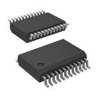
| TYPE | DESCRIPTION |
|---|
| Mounting Style | Surface Mount |
| Frequency | 100 MHz |
| Number of Pins | 24 Pin |
| Supply Voltage (DC) | 3.30 V |
| Case/Package | SSOP-24 |
| Number of Outputs | 10 Output |
| Supply Current | 25.0 mA |
| Number of Circuits | 1 Circuit |
| Power Dissipation | 0.65 W |
| Output Current Drive | -1.00 mA |
| Operating Temperature (Max) | 70 ℃ |
| Operating Temperature (Min) | 0 ℃ |
| Supply Voltage | 3V ~ 3.6V |
| Supply Voltage (Max) | 3.6 V |
| Supply Voltage (Min) | 3 V |
| TYPE | DESCRIPTION |
|---|
| Product Lifecycle Status | Active |
| Packaging | Tube |
| Size-Width | 5.3 mm |
| Operating Temperature | 0℃ ~ 70℃ |
The CDC351 is a high-performance clock-driver circuit that distributes one input (A) to ten outputs (Y) with minimum skew for clock distribution. The output-enable (OE)\ input disables the outputs to a high-impedance state. The CDC351 operates at nominal 3.3-V VCC.
●The propagation delays are adjusted at the factory using the P0 and P1 pins. The factory adjustments ensure that the part-to-part skew is minimized and is kept within a specified window. Pins P0 and P1 are not intended for customer use and should be connected to GND.
TI
1-Line to 10-Line 3.3V Clock Driver with Tri-State Outputs
TI
Clock Fanout Buffer 10Out 1IN 1:10 24Pin SSOP Tube
TI
Clock Fanout Buffer 10Out 1IN 1:10 24Pin SOIC Tube
TI
Clock Fanout Buffer 10Out 1IN 1:10 24Pin SOIC Tube
TI
Clock Fanout Buffer 10Out 1IN 1:10 24Pin SSOP Tube
TI
Clock Fanout Buffer 10Out 24Pin SOIC Clock Fanout Buffer 10Out 24Pin SOIC Clock Fanout Buffer 10Out 24Pin SOIC
TI
Clock Fanout Buffer 10Out 1IN 1:10 24Pin SSOP T/R
TI
Clock Fanout Buffer 10Out 1IN 1:10 24Pin SSOP T/R
TI
Clock Fanout Buffer 10Out 1IN 1:10 24Pin SOIC T/R
TI
Clock Fanout Buffer 10Out 1IN 1:10 24Pin SSOP T/R
Part Datasheet PDF Search
72,405,303 Parts Datasheet PDF, Update more than 5,000 PDF files ervery day.


