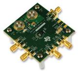
The CDCLVC1104EVM evaluation module is designed to demonstrate the electrical performance of the CDCLVC1104. The CDCLVC1104 is a high performance, low additive phase noise LVCMOS clock buffer. It has one LVCMOS input and four LVCMOS outputs. It also has an enable pin. For optimum performance, the board is equipped with 50ohm SMA connectors and well controlled 50ohm impedance microstrip transmission lines.
● Easy to use evaluation board to fan out Low phase noise LVCMOS clock signals
● Easy device setup
● Enable pin configurable through jumper and SMA
● Board powered at 2.5V or 3.3V
●It is important to operate this EVM within the input voltage range of 2.3V to 3.6V and the output voltage range of -0.5V to 3.6V .
TI
3.3V and 2.5V LVCMOS High-Performance Clock Buffer Family
TI
Clock Buffer, 250MHz, 2.3V to 3.6V, 4Outputs, TSSOP-8
TI
Clock Fanout Buffer 4Out 1IN 1:4 8Pin TSSOP Tube
TI
CDCLVC1104 Clock Buffer and Driver Evaluation Board
Part Datasheet PDF Search
72,405,303 Parts Datasheet PDF, Update more than 5,000 PDF files ervery day.


