Part Datasheet Search > Interface ICs > Intersil > HC55185CIM Datasheet PDF > HC55185CIM Datasheet Pages 18/20
HC55185CIM Datasheet - Intersil
| Manufacturer: | Intersil |
| Category: | Interface ICs |
| Case Package: | PLCC |
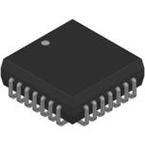
| Description: | SLIC 1CH 64dB 45mA 5V/-18V/-24V/-28V 28Pin PLCC |
| Pictures: |
HC55185CIMDatasheet PDF
Page:
of 20 Go
If the format of the manual is confusing, please download and read the original PDF file.

18
FN4831.15
February 9, 2012
Pin Descriptions
PLCC QFN SYMBOL DESCRIPTION
1 29 TIP TIP power amplifier output.
2 30 BGND Battery Ground - To be connected to zero potential. All loop current and longitudinal current flow from this ground.
Internally separate from AGND but it is recommended that it is connected to the same potential as AGND.
3 31 VBL Low battery supply connection.
4 32 VBH High battery supply connection for the most negative battery.
5 1 SW+ Uncommitted switch positive terminal.
6 2 SW- Uncommitted switch negative terminal.
73SWC
Switch control input. This TTL compatible input controls the uncommitted switch, with a logic “0” enabling the switch
and logic “1” disabling the switch. The logic control is disabled in the Power Denial state, forcing the switch to the open
state
8 4 F2 Mode Control Input - MSB. F2-F0 for the TTL compatible parallel control interface for controlling the various modes of
operation of the device.
9 5 F1 Mode control input.
10 6 F0 Mode control input.
11 7 E0 Detector Output Selection Input. This TTL input controls the multiplexing of the SHD (E0 = 1) and GKD (E0 = 0) comparator
outputs to the DET
output based upon the state at the F2-F0 pins (see the Device Operating Modes table shown on page 2).
12 9 DET Detector Output - This TTL output provides on-hook/off-hook status of the loop based upon the selected operating
mode. The detected output will either be switch hook, ground key or ring trip (see the Device Operating Modes table
shown on page 2).
13 10 ALM Thermal Shutdown Alarm. This pin signals the internal die temperature has exceeded safe operating temperature
(approximately 175°C) and the device has been powered down automatically.
14 11 AGND Analog ground reference. This pin should be externally connected to BGND.
15 12 BSEL Selects between high and low battery, with a logic “1” selecting the high battery and logic “0” the low battery.
16 13 TL Programming pin for the transient current limit feature, set by an external resistor to ground.
17 14 POL External capacitor on this pin sets the polarity reversal time.
18 15 VRS Ringing Signal Input - Analog input for driving 2-wire interface while in Ring Mode.
19 17 VRX Analog Receive Voltage - 4-wire analog audio input voltage. AC couples to CODEC.
20 18 VTX Transmit Output Voltage - Output of impedance matching amplifier, AC couples to CODEC.
21 19 VFB Feedback voltage for impedance matching. This voltage is scaled to accomplish impedance matching.
22 20 -IN Impedance matching amplifier summing node.
23 21 VCC Positive voltage power supply, usually +5V.
24 22 CDC DC Biasing Filter Capacitor - Connects between this pin and V
CC
.
25 23 RTD Ring trip filter network.
26 24 ILIM Loop Current Limit programming resistor.
27 25 RD Switch hook detection threshold programming resistor.
28 27 RING RING power amplifier output.
HC55185
Part Datasheet PDF Search
72,405,303 Parts Datasheet PDF, Update more than 5,000 PDF files ervery day.

