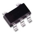
Part Datasheet Search > Voltage Regulators > Maxim Integrated > MAX8877EUK33+T Datasheet PDF > MAX8877EUK33+T Datasheet Pages 6/10
MAX8877EUK33+T Datasheet - Maxim Integrated
| Manufacturer: | Maxim Integrated |
| Category: | Voltage Regulators |
| Case Package: | SOT-23-5 |
| Description: | MAXIM INTEGRATED PRODUCTS MAX8877EUK33+T Fixed LDO Voltage Regulator, 2.5V to 6.5V In, 165mV Dropout, 3.3V/150mA Out, SOT-23-5 |
| Pictures: |
MAX8877EUK33+TDatasheet PDF
Page:
of 10 Go
If the format of the manual is confusing, please download and read the original PDF file.

MAX8877/MAX8878
_______________Detailed Description
The MAX8877/MAX8878 are low-noise, low-dropout,
low-quiescent-current linear regulators designed pri-
marily for battery-powered applications. The parts are
available with preset output voltages ranging from 1.5V
to 5V, in 100mV increments. These devices can supply
loads up to 150mA. As illustrated in Figure 1, the
MAX8877/MAX8878 consist of a 1.25V reference, error
amplifier, P-channel pass transistor, and internal feed-
back voltage divider.
The 1.25V bandgap reference is connected to the error
amplifier’s inverting input. The error amplifier compares
this reference with the feedback voltage and amplifies
the difference. If the feedback voltage is lower than the
reference voltage, the pass-transistor gate is pulled
lower, which allows more current to pass to the output
and increases the output voltage. If the feedback volt-
age is too high, the pass-transistor gate is pulled up,
allowing less current to pass to the output. The output
voltage is fed back through an internal resistor voltage
divider connected to the OUT pin.
An external bypass capacitor connected to the BP pin
reduces noise at the output. Additional blocks include a
current limiter, reverse battery protection, thermal sen-
sor, and shutdown logic. The MAX8878 also includes
an auto-discharge function, which actively discharges
the output voltage to ground when the device is placed
in shutdown mode.
Low-Noise, Low-Dropout, 150mA Linear
Regulators with '2982 Pinout
6 _______________________________________________________________________________________
SHUTDOWN
AND
POWER-ON
CONTROL
ERROR
AMP
1.25V
REF
P
N
*
OUT
BP
* AUTO-DISCHARGE, MAX8878 ONLY
GND
IN
SHDN
MAX8877
MAX8878
MOS DRIVER
WITH I
LIMIT
THERMAL
SENSOR
REVERSE
BATTERY
PROTECTION
Figure 1. Functional Diagram
______________________________________________________________Pin Description
PIN NAME FUNCTION
1IN
Regulator Input. Supply voltage can range from 2.5V to 6.5V. Bypass with a 1µF capacitor to GND
(see Capacitor Selection and Regulator Stability section).
2 GND
Ground. This pin also functions as a heatsink. Solder to a large pad or the circuit-board ground
plane to maximize power dissipation.
3 SHDN
Active-Low Shutdown Input. A logic low reduces the supply current to 10nA. On the MAX8878, a
logic low also causes the output voltage to discharge to GND. Connect to IN for normal operation.
4BP
Reference-Noise Bypass. Bypass with a low-leakage, 0.01µF ceramic capacitor for reduced noise at
the output.
5 OUT
Regulator Output. Sources up to 150mA. Bypass with a 1µF (<0.2Ω typical ESR) capacitor to GND
for V
OUT
≥ 2.5V and 3.3µF for V
OUT
< 2.5V.
Part Datasheet PDF Search
72,405,303 Parts Datasheet PDF, Update more than 5,000 PDF files ervery day.

