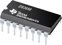
The DS3658 quad peripheral driver is designed for those applications where low operating power, high breakdown voltage, high output current and low output ON voltage are required. A unique input circuit combines TTL compatibility with high impedance. In fact, its extreme low input current allows it to be driven directly by a CMOS device.
●The outputs are capable of sinking 600 mA each and offer a 70V breakdown. However, for inductive loads the output should be clamped to 35V or less to avoid latch-up during turn off (inductive fly back protection—refer to AN-213 "SNOA610"). An on-chip clamp diode capable of handling 800 mA is provided at each output for this purpose. In addition, the DS3658 incorporates circuitry that specifies glitch-free power up or down operation and a fail-safe feature which puts the output in a high impedance state when the input is open.
●The PDIP package is specifically constructed to allow increased power dissipation over conventional packages. The four ground pins are directly connected to the device chip with a special cooper lead frame. When the quad driver is soldered into a PC board, the power rating of the device improves significantly.
● Single Saturated Transistor Outputs
● Low Standby Power, 10 mW Typical
● High Impedance TTL Compatible Inputs
● Outputs May Be Tied Together for Increased Current Capacity
● High Output Current
● 600 mA Per Output
● 2.4A Per Package
● No Output Latch-up at 35V
● Low Output ON Voltage (350 mV typ @ 600 mA)
● High Breakdown Voltage (70V)
● Open Collector Outputs
● Output Clamp Diodes for Inductive Fly Back Protection
● NPN Inputs for Minimal Input Currents (1 µA Typical)
● Low Operating Power
● Standard 5V Power Supply
● Power Up/Down Protection
● Fail Safe Operation
● 2W Power Package
● Pin-for-Pin Compatible with SN75437
●All trademarks are the property of their respective owners.


