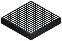
Part Datasheet Search > Microcontrollers > NXP > LPC4330FET256,551 Datasheet PDF
LPC4330FET256,551 Datasheet PDF - NXP
| Manufacturer: | NXP |
| Category: | Microcontrollers |
| Case Package: | LBGA-256 |
| Description: | MCU 32Bit ARM Cortex M4 RISC ROMLess 2.5V/3.3V 256Pin LBGA Tray |
| Documentation: | LPC4330FET256,551 Datasheet (2 Pages)LPC4330FET256,551 User Reference Manual Guide (1442 Pages) |
| Pictures: |
LPC4330FET256,551 Datasheet PDF
ADatasheet has not yet included the datasheet for LPC4330FET256,551
If necessary, please send a supplementary document request to the administrator

LPC4330FET256,551 Datasheet PDF (2 Pages)
LPC4330FET256,551 Specifications
| TYPE | DESCRIPTION |
|---|---|
| Mounting Style | Surface Mount |
| Frequency | 204 MHz |
| Number of Pins | 256 Pin |
| Supply Voltage (DC) | 2.20V (min) |
| Case/Package | LBGA-256 |
| Number of Positions | 256 Position |
| Clock Speed | 204 MHz |
| RAM Memory Size | 264 KB |
| Number of Bits | 32 Bit |
| Power Dissipation | 1500 mW |
| FLASH Memory Size | 0 kB |
| Number of ADCs | 1 ADC |
| Number of Inputs and Outputs | 164 Input |
| Operating Temperature (Max) | 85 ℃ |
| Operating Temperature (Min) | -40 ℃ |
| Power Dissipation (Max) | 1500 mW |
| Number of DACs | 1 DAC |
| Supply Voltage | 3.6 V |
| Supply Voltage (Max) | 3.6 V |
| Supply Voltage (Min) | 2.2 V |
LPC4330FET256,551 Size & Package
| TYPE | DESCRIPTION |
|---|---|
| Product Lifecycle Status | Active |
| Packaging | Tray |
| Size-Length | 17.2 mm |
| Size-Width | 17.2 mm |
| Size-Height | 1.1 mm |
| Operating Temperature | -40℃ ~ 85℃ |
LPC4330FET256,551 Environmental
LPC4330FET256,551 Function Overview
Overview
●The LPC4330FET256 is an ARM Cortex-M4 based digital signal controller with an ARM Cortex-M0 coprocessor designed for embedded applications requiring signal processing. The ARM Cortex-M4 core offers single-cycle Multiply-Accumulate and SIMD instructions and a hardware floating-point unit to support signal processing while the M0 coprocessor handles I/O and digital control processing. The LPC4330FET256 includes 264 kB of data memory, two High Speed USB 2.0 Host/OTG/Devices, advanced configurable peripherals such as the State Configurable Timer (SCT), Serial General Purpose I/O (SGPIO), and SPI Flash Interface (SPIFI) as well as Ethernet, an external memory controller and multiple digital and analog peripherals.
●MoreLess
●## Features
● ARM Cortex-M4 processor, running at frequencies of up to 204 MHz
● ARM Cortex-M4 built-in Memory Protection Unit (MPU) supporting eight regions
● ARM Cortex-M4 built-in Nested Vectored Interrupt Controller (NVIC)
● Hardware floating-point unit
● Non-maskable Interrupt (NMI) input
● JTAG and Serial Wire Debug (SWD)
● System tick timer
● ARM Cortex-M0 co-processor running at frequencies of up to 204 MHz
● 200 kB SRAM for code and data use
● Two 32 kB SRAM blocks with separate bus access
● 32 kB ROM containing boot code and on-chip software drivers
● 32 bit One-Time Programmable (OTP) memory for customer use
● Serial GPIO (SGPIO) interface
● State Configurable Timer (SCT) subsystem on AHB
● Quad SPI Flash Interface (SPIFI) with four lanes and up to 40 MB per second
● 10/100T Ethernet MAC with RMII and MII interfaces and DMA support
● One High-speed USB 2.0 Host/Device/OTG interface with DMA support
● One High-speed USB 2.0 Host/Device interface with DMA support
● One 550 UART with DMA support and full modem interface
● Three 550 USARTs with DMA and synchronous mode support
● One C_CAN 2.0B controller with one channel
● Two SSP controllers with FIFO and multi-protocol support
● One SPI controller
● One Fast-mode Plus I2C-bus interface with rates of up to 1 Mbit/s
● One Fast-mode I2C-bus interface
● Two I2S interfaces
● External Memory Controller (EMC) supporting external SRAM, ROM, flash, SDRAM
● Secure Digital Input Output (SDIO) card interface
● Eight-channel General-Purpose DMA (GPDMA) controller
● Up to 146 General-Purpose Input/Output (GPIO) pins
● Four general-purpose timer/counters with capture and match capabilities
● One motor control Pulse Width Modulator (PWM) for three-phase motor control
● One Quadrature Encoder Interface (QEI)
● Repetitive Interrupt timer (RI timer)
● Windowed watchdog timer (WWDT)
● Ultra-low power Real-Time Clock (RTC) on separate power domain
● Alarm timer; can be battery powered
● One 10-bit DAC with DMA support and a data conversion rate of 400 kSamples/s
● Two 10-bit ADCs with DMA support and a data conversion rate of 400 kSamples/s
● Two 128-bit secure OTP memories for AES key storage and customer use
● Crystal oscillator with an operating range of 1 MHz to 25 MHz
● 12 MHz Internal RC (IRC) oscillator trimmed to 1 % accuracy
● Ultra-low power Real-Time Clock (RTC) crystal oscillator
● Three PLLs allow CPU operation up to the maximum CPU rate
● Clock output
● Single 3.3 V (2.2 V to 3.6 V) power supply with on-chip DC-to-DC converter
● RTC power domain can be powered separately by a 3 V battery supply
● Four reduced power modes
● Processor wake-up from Sleep mode via wake-up interrupts
● Brownout detect with four separate thresholds for interrupt and forced reset
● Power-On Reset (POR)
● see selection guide for features per type
●## Target Applications
● Industrial
● Consumer
● White goods
● RFID readers
● e-Metering
●## Features
show more
LPC4330FET256,551 Documents
LPC4330 Documents
NXP
LPC4330FET180 - Dual-core Cortex-M4/M0, 264KB SRAM, 2 HS USB with on-chip PHY, Ethernet, CAN, AES, SPIFI, SGPIO, SCT BGA 180Pin
NXP
MCU 32Bit LPC4300 ARM Cortex M4 RISC ROMLess 2.5V/3.3V 100Pin TFBGA T/R
NXP
Dual-core Cortex-M4/M0, 264KB SRAM, 2 HS USB with on-chip PHY, Ethernet, CAN, AES, SPIFI, SGPIO, SCT
Part Datasheet PDF Search
Example: STM32F103
72,405,303 Parts Datasheet PDF, Update more than 5,000 PDF files ervery day.
Relate Parts
Relate Documentations: LPC4330 Datasheet

