Description
●The TMS570LS series is a high performance automotive grade microcontroller family which has been certified for use in IEC 61508 SIL3 safety systems. The safety architecture includes Dual CPUs in lockstep, CPU and Memory Built-In Self Test (BIST) logic, ECC on both the Flash and the data SRAM, parity on peripheral memories, and loop back capability on peripheral IOs.
●The TMS570LS family integrates the ARMç Cortexâ-R4F Floating Point CPU which offers an efficient 1.6 DMIPS/MHz, and has configurations which can run up to 160 MHz providing more than 250 DMIPS. The TMS570LS series also provides different Flash (1MB or 2MB) and data SRAM (128KB or 160KB) options with single bit error correction and double bit error detection.
●Features
●• High-Performance Automotive Grade Microcontroller for Safety Critical Applications
● – Certified for use in SIL3 Applications
● – Dual CPUs running in Lockstep
● – ECC on Flash and SRAM
● – CPU and Memory BIST (Built-In Self Test)
● – Error Signaling Module (ESM) w/ Error Pin
●• ARM® Cortex™-R4F 32-Bit RISC CPU
● – Efficient 1.6 DMIPS/MHz with 8-stage pipeline
● – Floating Point Unit with Single/Double Precision
● – Memory Protection Unit (MPU)
● – Open Architecture With Third-Party Support
●• Operating Features
● – Up to 160-MHz System Clock
● – Core Supply Voltage (VCC): 1.5 V
● – I/O Supply Voltage (VCCIO): 3.3 V
●• Integrated Memory
● – 1M-Byte or 2M-Byte Flash with ECC
● – 128K-Byte or 160K-Byte RAM with ECC
●• Multiple Communication interfaces including FlexRay, CAN, and LIN
●• NHET Timer and 2x 12-bit ADCs
●• External Memory Interface (EMIF)
● – 16bit Data, 22bit Address, 4 Chip Selects
●• Common TMS470/570 Platform Architecture
● – Consistent Memory Map across the family
● – Real-Time Interrupt (RTI) OS Timer
● – Vectored Interrupt Module (VIM)
● – Cyclic Redundancy Checker (CRC, 2 Channels)
●• Direct Memory Access (DMA) Controller
● – 32 DMA requests and 16 Channels/ Control Packets
● – Parity on Control Packet Memory
● – Dedicated Memory Protection Unit (MPU)
●• Frequency-Modulated Zero-Pin Phase-Locked Loop (FMzPLL)-Based Clock Module
● – Oscillator and PLL clock monitor
●• Up to 115 Peripheral IO pins
● – 16 Dedicated GIO - 8 w/ External Interrupts
● – Programmable External Clock (ECLK)
●• Communication Interfaces
● – Three Multi-buffered Serial Peripheral Interface (MibSPI) each with:
●• Four Chip Selects and one Enable pin
●• 128 buffers with parity
●• One with parallel mode
● – Two UART (SCI) interfaces with Local Interconnect Network Interface (LIN 2.0)
● – Three CAN (DCAN) Controller
●• Two with 64 mailboxes, one with 32
●• Parity on mailbox RAM
● – Dual Channel FlexRay™ Controller
●• 8K-Byte message RAM with parity
●• Transfer Unit with MPU and parity
●• High-End Timer (NHET)
● – 32 Programmable I/O Channels
● – 128 Words High-End Timer RAM with parity
● – Transfer Unit with MPU and parity
●• Two 12-Bit Multi-Buffered ADCs (MibADC)
● – 24 total ADC Input channels
● – Each has 64 Buffers with parity
●• Trace and Calibration Interfaces
● – Embedded Trace Module (ETMR4)
● – Data Modification Module (DMM)
● – RAM Trace Port (RTP)
● – Parameter Overlay Module (POM)
●• On-Chip emulation logic including IEEE 1149.1 JTAG, Boundary Scan and ARM Coresight components
●• Full Development Kit Available
● – Development Boards
● – Code Composer Studio Integrated Development Environment (IDE)
● – HaLCoGen Code Generation Tool
● – HET Assembler and Simulator
● – nowFlash Flash Programming Tool
●• Packages Supported
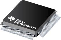
● – 144-Pin Quad Flat Pack (PGE) [Green]
● – 337-Pin Ball Grid Array (ZWT) [Green]
●• Community Resources
● – TI E2E Community


