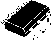
The SN74LVC1G373DCKR is a single D Latch designed for 1.65 to 5.5V VCC operation. It is particularly suitable for implementing buffer registers, I/O ports, bidirectional bus drivers and working registers. While the LE input is high, the Q outputs follow the data (D) inputs. When LE is taken low, the Q outputs are latched at the logic levels set up at the D inputs. While the LE input is high, the Q output follows the data (D) input. When LE is taken low, the Q output is latched at the logic level set up at the D input. OE\ does not affect the internal operations of the latch. Old data can be retained or new data can be entered while the outputs are in the high-impedance state. A buffered OE\ input can be used to place the output in either a normal logic state (high or low logic levels) or the high-impedance state. In the high-impedance state, the output neither loads nor drives the bus lines significantly.
● Provides down translation to VCC
● Maximum tpd of 4ns at 3.3V
● Ioff Supports live insertion, partial-power-down mode and back drive protection
● Latch-up performance exceeds 100mA per JESD, 78 class II
● 10µA Maximum low power consumption
● ±24mA Output drive at 3.3V
● Green product and no Sb/Br


