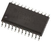
The SN74LVC4245ADWR is a 8-bit (octal) Non-inverting Bus Transceiver contains two separate supply rails, B port has VCCB, which is set at 3.3V and A port has VCCA, which is set at 5V. This allows for translation from a 3.3 to a 5V environment and vice versa. The SN74LVC4245ADWR device is designed for asynchronous communication between data buses. The device transmits data from the A bus to the B bus or from the B bus to the A bus, depending on the logic level at the direction-control (DIR) input. The output-enable (OE) input can be used to disable the device so the buses are effectively isolated. The control circuitry (DIR, OE) is powered by VCCA. The SN74LVC4245ADWR device terminal out allows the designer to switch to a normal all-3.3V or all-5V 20-terminal SN74LVC4245ADWR device without board re-layout. The designer uses the data paths for pins 2-11 and 14-23 of the SN74LVC4245ADWR device to align with the conventional "245 terminal out.
● Bidirectional voltage translator
● 5.5V on A port and 2.7 to 3.6V on B port
● Control inputs VIH/VIL levels are referenced to VCCA voltage
● Latch-up performance exceeds 250mA per JESD 17
● Green product and no Sb/Br
●Device has limited built-in ESD protection. The leads should be shorted together or the device placed in conductive foam during storage or handling to prevent electrostatic damage to the MOS gates.


