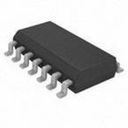
description/ordering information
●This bus buffer is designed specifically for low-voltage (3.3-V) VCC operation, but with the capability to provide a TTL interface to a 5-V system environment.
●The SN74LVT125 features independent line drivers with 3-state outputs. Each output is in the high-impedance state when the associated output-enable (OE) input is high.
●Active bus-hold circuitry holds unused or undriven inputs at a valid logic state. Use of pullup or pulldown resistors with the bus-hold circuitry is not recommended.
●This device is fully specified for partial-power-down applications using Ioff. The Ioff circuitry disables the outputs, preventing damaging current backflow through the device when it is powered down.
●• Supports Mixed-Mode Signal Operation
● (5-V Input and Output Voltages With 3.3-V VCC)
●• Supports Unregulated Battery Operation Down to 2.7 V
●• Typical VOLP (Output Ground Bounce)
● <0.8 V at VCC = 3.3 V, TA = 25°C
●• Ioff Supports Partial-Power-Down Mode Operation
●• Bus-Hold Data Inputs Eliminate the Need for External Pullup Resistors
●• Latch-Up Performance Exceeds 500 mA Per JEDEC Standard JESD-17
●• ESD Protection Exceeds JESD 22
● − 2000-V Human-Body Model (A114-A)
● − 200-V Machine Model (A115-A)


