| TYPE | DESCRIPTION |
|---|
| Mounting Style | Surface Mount |
| Number of Pins | 10 Pin |
| Case/Package | VSON-10 |
| Number of Outputs | 1 Output |
| Output Voltage | 1.8V ~ 5.5V |
| Output Current | 1.2 A |
| Number of Positions | 10 Position |
| Quiescent Current | 50.0 µA |
| Number of Regulated Outputs | 1 Output |
| Switching Frequency | 1.65 MHz |
| Topology | Boost |
| Input Voltage (Max) | 5.5 V |
| Input Voltage (Min) | 0.3 V |
| Output Voltage (Max) | 5.5 V |
| Output Voltage (Min) | 1.8 V |
| Output Current (Max) | 0.6 A |
| Operating Temperature (Max) | 85 ℃ |
| Operating Temperature (Min) | -40 ℃ |
| Supply Voltage | 0.3 V |
| Input Voltage | 0.3V ~ 5.5V |
| TYPE | DESCRIPTION |
|---|
| Product Lifecycle Status | Active |
| Packaging | Tape & Reel (TR) |
| Operating Temperature | -40℃ ~ 85℃ (TA) |
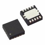
The TPS6120x devices provide a power supply solution for products powered by either a single-cell, two-cell, or three-cell alkaline, NiCd or NiMH, or one-cell Li-Ion or Li-polymer battery. It is also used in fuel cell or solar cell powered devices where the capability of handling low input voltages is essential. Possible output currents depend on the input to output voltage ratio. The devices provide output currents of up to 600 mA at a 5-V output, while using a single-cell Li-Ion or Li-Polymer battery and discharges it down to 2.6 V. The boost converter is based on a fixed frequency, pulse-width-modulation (PWM) controller using synchronous rectification to obtain maximum efficiency. At low load currents, the converter enters the Power Save mode to maintain a high efficiency over a wide load current range. The Power Save mode can be disabled, forcing the converter to operate at a fixed switching frequency. The average input current is limited to a maximum value of 1500 mA. The output voltage is programmed by an external resistor divider, or is fixed internally on the chip. The converter can be disabled to minimize battery drain. During shutdown, the load is completely disconnected from the battery. The device is packaged in a 10-pin VSON package measuring 3 mm × 3 mm.
TI
0.3V Input Voltage Boost Converter with 1.3A Switches and Down Mode in 3x3 QFN
TI
Step-Up Regulator 0.3V Input Voltage Boost Converter with 1.3A Switches and 'Down Mode' in 3x3 QFN Conv DC-DC Single Step Up 0.3V to 5.5V 10Pin VSON EP T/R
TI
Step-Up Regulator 0.3V Input Voltage Boost Converter with 1.3A Switches and 'Down Mode' in 3x3 QFN Conv DC-DC 0.3V to 5.5V Step Up Single-Out 1.8V to 5.5V 0.6A 10Pin VSON EP T/R
TI
Evaluation Module for 0.3V Input Voltage Boost Converter with 1.3A Switches
TI
0.3V Input Voltage Boost Converter with 1.3A Switches and 'Down Mode' in 3x3 QFN 10-VSON -40℃ to 85℃
TI
0.3V Input Voltage Boost Converter with 1.3A Switches and 'Down Mode' in 3x3 QFN 10-VSON -40℃ to 85℃
Part Datasheet PDF Search
72,405,303 Parts Datasheet PDF, Update more than 5,000 PDF files ervery day.


