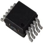
The TSB81BA3E provides the digital and analog transceiver functions needed to implement a three-port node in a cable-based IEEE 1394 network. Each cable port incorporates two differential line transceivers. The transceivers include circuitry to monitor the line conditions as needed for determining connection status, for initialization and arbitration, and for packet reception and transmission. The TSB81BA3E is designed to interface with a link-layer controller (LLC), such as the TSB82AA2, TSB12LV21, TSB12LV26, TSB12LV32, TSB42AA4, TSB42AB4, TSB12LV01B, or TSB12LV01C. It also may be connected cable port to cable port to an integrated 1394 Link + PHY layer such as the TSB43AB2.
●The TSB81BA3E can be powered by a single 3.3-V supply when the VREG_PD terminal (terminal 73 on the PFP package and terminal B7 on the ZAJ package) is tied to GND. VREG_PD enables the internal 3.3-V to 1.95-V regulator which provides the 1.95-V to the core. The When VREG_PD is pulled high to VDD through at least a 1-kΩ resistor the TSB81BA3E internal regulator is off and the device can be powered by two separate external regulated supplies: 3.3-V for the I/Os and 1.95-V for the core. The core voltage is supplied to the PLLVDD-CORE and DVDD-CORE terminals to the requirements in the recommended operating conditions (1.95-V nominal). The PLLVDD-CORE terminals must be separated from the DVDD-CORE terminals. The PLLVDD-CORE and the DVDD-CORE terminals must be decoupled with 1 uF capacitors to stabilze the respective supply. Additional 0.10 µF and 0.01 µF high-frequency bypass capacitors may also be used. The separation between DVDD-CORE and PLLVDD-CORE may be implemented by separate power supply rails, or by a single power supply rail, where the DVDD-CORE and PLLVDD-CORE are separated by a filter network to keep noise from the PLLVDD-CORE supply.
●The TSB81BA3E requires an external 98.304-MHz crystal oscillator to generate a reference clock. The external clock drives an internal phase-locked loop (PLL), which generates the required reference signal. This reference signal provides the clock signals that control transmission of the outbound encoded information. A 49.152-MHz clock signal is supplied to the associated LLC for synchronization of the two devices and is used for resynchronization of the received data when operating the PHY-link interface in compliance with the IEEE 1394a-2000 standard. A 98.304-MHz clock signal is supplied to the associated LLC for synchronization of the two devices when operating the PHY-link interface in compliance with the IEEE P1394b standard. The power down (PD) function, when enabled by asserting the PD terminal high, stops operation of the PLL.


