
Part Datasheet Search > Latches > TI > CD74HCT373M Datasheet PDF > CD74HCT373M Datasheet Pages 1/10
CD74HCT373M Datasheet - TI
| Manufacturer: | TI |
| Category: | Latches |
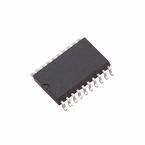
| Case Package: | SOIC-20 |
| Description: | Latch Transparent 3-ST 8CH D-Type 20Pin SOIC Tube |
| Pictures: |
CD74HCT373MDatasheet PDF
Page:
of 10 Go
If the format of the manual is confusing, please download and read the original PDF file.

© 2005 Fairchild Semiconductor Corporation DS005367 www.fairchildsemi.com
February 1984
Revised May 2005
MM74HCT373 • MM74HCT374 3-STATE Octal D-Type Latch • 3-STATE Octal D-Type Flip-Flop
MM74HCT373 • MM74HCT374
3-STATE Octal D-Type Latch •
3-STATE Octal D-Type Flip-Flop
General Description
The MM74HCT373 octal D-type latches and
MM74HCT374 Octal D-type flip flops advanced silicon-gate
CMOS technology, which provides the inherent benefits of
low power consumption and wide power supply range, but
are LS-TTL input and output characteristic & pin-out com-
patible. The 3-STATE outputs are capable of driving 15 LS-
TTL loads. All inputs are protected from damage due to
static discharge by internal diodes to V
CC
and ground.
When the MM74HCT373 LATCH ENABLE input is HIGH,
the Q outputs will follow the D inputs. When the LATCH
ENABLE goes LOW, data at the D inputs will be retained at
the outputs until LATCH ENABLE returns HIGH again.
When a high logic level is applied to the OUTPUT CON-
TROL input, all outputs go to a high impedance state,
regardless of what signals are present at the other inputs
and the state of the storage elements.
The MM74HCT374 are positive edge triggered flip-flops.
Data at the D inputs, meeting the setup and hold time
requirements, are transferred to the Q outputs on positive
going transitions of the CLOCK (CK) input. When a high
logic level is applied to the OUTPUT CONTROL (OC)
input, all outputs go to a high impedance state, regardless
of what signals are present at the other inputs and the state
of the storage elements.
MM74HCT devices are intended to interface between TTL
and NMOS components and standard CMOS devices.
These parts are also plug in replacements for LS-TTL
devices and can be used to reduce power consumption in
existing designs.
Features
■ TTL input characteristic compatible
■ Typical propagation delay: 20 ns
■ Low input current: 1
P
A maximum
■ Low quiescent current: 80
P
A maximum
■ Compatible with bus-oriented systems
■ Output drive capability: 15 LS-TTL loads
Ordering Code:
Devices also available in Tape and Reel. Specify by appending the suffix letter “X” to the ordering code.
Order Number Package Number Package Descriptions
MM74HCT373WM M20B 20-Lead Small Outline Integrated Circuit (SOIC), JEDEC MS-013, 0.300" Wide
MM74HCT373SJ M20D 20-Lead Small Outline Package (SOP), EIAJ TYPE II, 5.3mm Wide
MM74HCT373MTC MTC20 20-Lead Thin Shrink Small Outline Package (TSSOP), JEDEC MO-153, 4.4mm Wide
MM74HCT373N N20A 20-Lead Plastic Dual-In-Line Package (PDIP), JEDEC MS-001, 0.300" Wide
MM74HCT374WM M20B 20-Lead Small Outline Integrated Circuit (SOIC), JEDEC MS-013, 0.300" Wide
MM74HCT374SJ M20D 20-Lead Small Outline Package (SOP), EIAJ TYPE II, 5.3mm Wide
MM74HCT374MTC MTC20 20-Lead Thin Shrink Small Outline Package (TSSOP), JEDEC MO-153, 4.4mm Wide
MM74HCT374N N20A 20-Lead Plastic Dual-In-Line Package (PDIP), JEDEC MS-001, 0.300" Wide
Part Datasheet PDF Search
72,405,303 Parts Datasheet PDF, Update more than 5,000 PDF files ervery day.